|
|
|
|
11.0. Test Results: Part B |
|
|
|
|
|
11.0. Test Results: Part B |
|
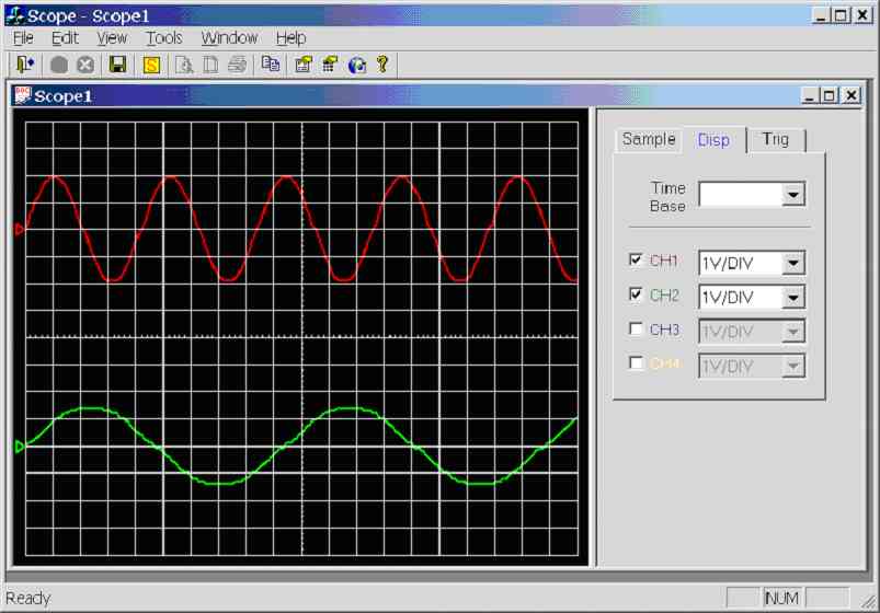 Figure 11.3.1a.
Screen dump of scope program (Dual Channel Test)
Figure 11.3.1a.
Screen dump of scope program (Dual Channel Test)
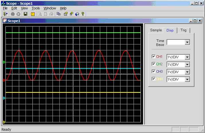 Figure 11.3.2a.
Screen dump of scope program (sample rate = 1 kHz, CH1 = 25Hz sinewave, CH2 =
5V, CH3 = 5V, CH4 = 5V)
25Hz
sinewave (0-5V) connected to CH2/AN1 and all other channels connected to 5V,
see figure 11.3.2b. 4 divisions per cycle, hence the calculated channel 2
frequency is 1/(4*0.01) = 25Hz. Channels 1, 3 & 4 are at 5V DC.
Figure 11.3.2a.
Screen dump of scope program (sample rate = 1 kHz, CH1 = 25Hz sinewave, CH2 =
5V, CH3 = 5V, CH4 = 5V)
25Hz
sinewave (0-5V) connected to CH2/AN1 and all other channels connected to 5V,
see figure 11.3.2b. 4 divisions per cycle, hence the calculated channel 2
frequency is 1/(4*0.01) = 25Hz. Channels 1, 3 & 4 are at 5V DC.
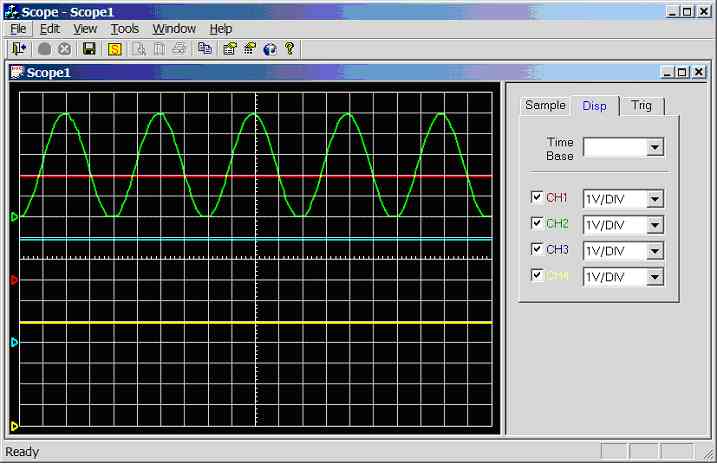 Figure 11.3.2b.
Screen dump of scope program (sample rate = 1 kHz, CH2 = 25Hz sinewave, CH1 =
5V, CH3 = 5V, CH4 = 5V)
25Hz
sinewave (0-5V) connected to CH3/AN2 and all other channels connected to 5V,
see figure 11.3.2c. 4 divisions per cycle, hence the calculated channel 3
frequency is 1/(4*0.01) = 25Hz. Channels 1, 2 & 4 are at 5V DC.
Figure 11.3.2b.
Screen dump of scope program (sample rate = 1 kHz, CH2 = 25Hz sinewave, CH1 =
5V, CH3 = 5V, CH4 = 5V)
25Hz
sinewave (0-5V) connected to CH3/AN2 and all other channels connected to 5V,
see figure 11.3.2c. 4 divisions per cycle, hence the calculated channel 3
frequency is 1/(4*0.01) = 25Hz. Channels 1, 2 & 4 are at 5V DC.
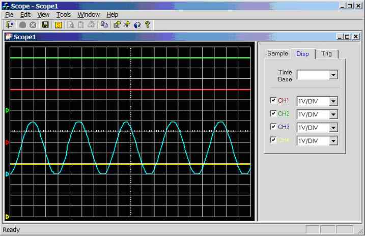 Figure 11.3.2c.
Screen dump of scope program (sample rate = 1 kHz, CH3 = 25Hz sinewave, CH1 =
5V, CH2 = 5V, CH4 = 5V)
25Hz
sinewave (0-5V) connected to CH4/AN3 and all other channels connected to 5V,
see figure 11.3.2d. 4 divisions per cycle, hence the calculated channel 4
frequency is 1/(4*0.01) = 25Hz. Channels 1, 2 & 3 are at 5V DC.
Figure 11.3.2c.
Screen dump of scope program (sample rate = 1 kHz, CH3 = 25Hz sinewave, CH1 =
5V, CH2 = 5V, CH4 = 5V)
25Hz
sinewave (0-5V) connected to CH4/AN3 and all other channels connected to 5V,
see figure 11.3.2d. 4 divisions per cycle, hence the calculated channel 4
frequency is 1/(4*0.01) = 25Hz. Channels 1, 2 & 3 are at 5V DC.
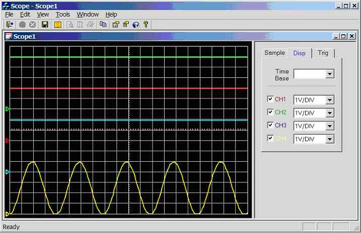 Figure 11.3.2d.
Screen dump of scope program (sample rate = 1 kHz, CH4 = 25Hz sinewave, CH1 =
5V, CH2 = 5V, CH3 = 5V)
11.3.2.1. Dual Channel Operation Using Two Signal Generators
Fluke
PM5139 function generator (calibrated) connected to
channel 1 (red), Thandar TG 101 function generator (not calibrated)
connected to channel 2 (green). Sample rate
is 1000Hz (scope time-base is 0.01).
Channel 1
connected to 10Hz sine-wave (5Vpp), channel 2
connected to 30Hz sine-wave (4Vpp), see figure 11.3.2.1a.
Channel 1: 10 divisions per cycle, hence the
calculated frequency is 1/(10*0.01) = 10Hz. Channel
2: 4.2 divisions per cycle, hence the calculated frequency is
1/(4.2*0.01) = 23.8 Hz (note channel 2 signal generator is not calibrated,
this is the true frequency).
Figure 11.3.2d.
Screen dump of scope program (sample rate = 1 kHz, CH4 = 25Hz sinewave, CH1 =
5V, CH2 = 5V, CH3 = 5V)
11.3.2.1. Dual Channel Operation Using Two Signal Generators
Fluke
PM5139 function generator (calibrated) connected to
channel 1 (red), Thandar TG 101 function generator (not calibrated)
connected to channel 2 (green). Sample rate
is 1000Hz (scope time-base is 0.01).
Channel 1
connected to 10Hz sine-wave (5Vpp), channel 2
connected to 30Hz sine-wave (4Vpp), see figure 11.3.2.1a.
Channel 1: 10 divisions per cycle, hence the
calculated frequency is 1/(10*0.01) = 10Hz. Channel
2: 4.2 divisions per cycle, hence the calculated frequency is
1/(4.2*0.01) = 23.8 Hz (note channel 2 signal generator is not calibrated,
this is the true frequency).
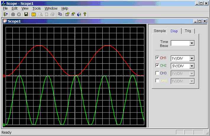 Figure 11.3.2.1a.
Screen dump of scope program (sample rate = 1 kHz, CH1 = 10Hz sinewave, CH2 =
30Hz sinewave)
Figure 11.3.2.1a.
Screen dump of scope program (sample rate = 1 kHz, CH1 = 10Hz sinewave, CH2 =
30Hz sinewave)
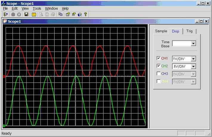 Figure 11.3.2.1b.
Screen dump of scope program (sample rate = 1 kHz, CH1 = 25Hz sinewave, CH2 =
30Hz sinewave)
Channel 1
connected to 25Hz sine-wave (5Vpp), channel 2
connected to 30Hz sine-wave (4Vpp), see figure 11.3.2.1b.
Channel 1: 4 divisions per cycle, hence the
calculated frequency is 1/(4*0.01) = 25Hz. Channel 2
unaffected.
Figure 11.3.2.1b.
Screen dump of scope program (sample rate = 1 kHz, CH1 = 25Hz sinewave, CH2 =
30Hz sinewave)
Channel 1
connected to 25Hz sine-wave (5Vpp), channel 2
connected to 30Hz sine-wave (4Vpp), see figure 11.3.2.1b.
Channel 1: 4 divisions per cycle, hence the
calculated frequency is 1/(4*0.01) = 25Hz. Channel 2
unaffected.
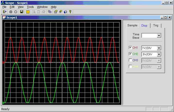 Figure 11.3.2.1c.
Screen dump of scope program (sample rate = 1 kHz, CH1 = 50Hz sinewave, CH2 =
30Hz sinewave)
Channel 1
connected to 50Hz sine-wave (5Vpp), channel 2
connected to 30Hz sine-wave (4Vpp), see figure 11.3.2.1c.
Channel 1: 2 divisions per cycle, hence the calculated frequency is
1/(2*0.01) = 50Hz. Channel 2 unaffected.
Figure 11.3.2.1c.
Screen dump of scope program (sample rate = 1 kHz, CH1 = 50Hz sinewave, CH2 =
30Hz sinewave)
Channel 1
connected to 50Hz sine-wave (5Vpp), channel 2
connected to 30Hz sine-wave (4Vpp), see figure 11.3.2.1c.
Channel 1: 2 divisions per cycle, hence the calculated frequency is
1/(2*0.01) = 50Hz. Channel 2 unaffected.
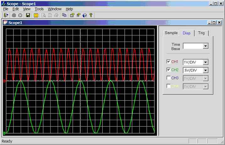 Figure 11.3.2.1d.
Screen dump of scope program (sample rate = 1 kHz, CH1 = 100Hz sinewave, CH2 =
30Hz sinewave)
Channel 1
connected to 100Hz sine-wave (5Vpp), channel 2
connected to 30Hz sine-wave (4Vpp), see figure 11.3.2.1d.
Channel 1: 1 divisions per cycle, hence the
calculated frequency is 1/(1*0.01) = 100Hz. Channel
2 unaffected.
Figure 11.3.2.1d.
Screen dump of scope program (sample rate = 1 kHz, CH1 = 100Hz sinewave, CH2 =
30Hz sinewave)
Channel 1
connected to 100Hz sine-wave (5Vpp), channel 2
connected to 30Hz sine-wave (4Vpp), see figure 11.3.2.1d.
Channel 1: 1 divisions per cycle, hence the
calculated frequency is 1/(1*0.01) = 100Hz. Channel
2 unaffected.
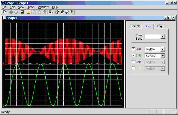 Figure 11.3.2.1e.
Screen dump of scope program (sample rate = 1 kHz, CH1 = 500Hz sinewave, CH2 =
30Hz sinewave)
Channel 1
connected to 500Hz sine-wave (5Vpp), channel 2
connected to 30Hz sine-wave (4Vpp), see figure 11.3.2.1e.
Channel 1: Under sampled, aliasing has occurred.
Channel 2 unaffected.
Figure 11.3.2.1e.
Screen dump of scope program (sample rate = 1 kHz, CH1 = 500Hz sinewave, CH2 =
30Hz sinewave)
Channel 1
connected to 500Hz sine-wave (5Vpp), channel 2
connected to 30Hz sine-wave (4Vpp), see figure 11.3.2.1e.
Channel 1: Under sampled, aliasing has occurred.
Channel 2 unaffected.
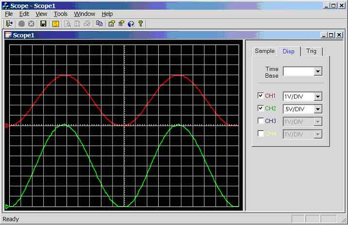 Figure 11.3.2.1f.
Screen dump of scope program (sample rate = 1 kHz, CH1 = 500Hz sinewave, CH2 =
30Hz sinewave)
Channel 1
connected to 10Hz sine-wave (5Vpp), channel 2
connected to 10Hz sine-wave (4Vpp), see figure 11.3.2.1f.
Channel 1: 10 divisions per cycle, hence the
calculated frequency is 1/(10*0.01) = 10Hz. Channel
2: 4.2 divisions per cycle, hence the calculated frequency is
1/(10*0.01) = 10 Hz
Figure 11.3.2.1f.
Screen dump of scope program (sample rate = 1 kHz, CH1 = 500Hz sinewave, CH2 =
30Hz sinewave)
Channel 1
connected to 10Hz sine-wave (5Vpp), channel 2
connected to 10Hz sine-wave (4Vpp), see figure 11.3.2.1f.
Channel 1: 10 divisions per cycle, hence the
calculated frequency is 1/(10*0.01) = 10Hz. Channel
2: 4.2 divisions per cycle, hence the calculated frequency is
1/(10*0.01) = 10 Hz
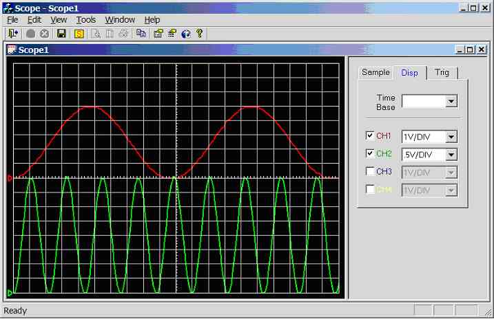 Figure 11.3.2.1g.
Screen dump of scope program (sample rate = 1 kHz, CH1 = 10Hz sinewave, CH2 =
50Hz sinewave)
Channel 1
connected to 10Hz sine-wave (5Vpp), channel 2
connected to 50Hz sine-wave (4Vpp), see figure 11.3.2.1g.
Channel 1: unaffected.
Channel 2: 2 divisions per cycle, hence the
calculated frequency is 1/(2*0.01) = 50 Hz.
Figure 11.3.2.1g.
Screen dump of scope program (sample rate = 1 kHz, CH1 = 10Hz sinewave, CH2 =
50Hz sinewave)
Channel 1
connected to 10Hz sine-wave (5Vpp), channel 2
connected to 50Hz sine-wave (4Vpp), see figure 11.3.2.1g.
Channel 1: unaffected.
Channel 2: 2 divisions per cycle, hence the
calculated frequency is 1/(2*0.01) = 50 Hz.
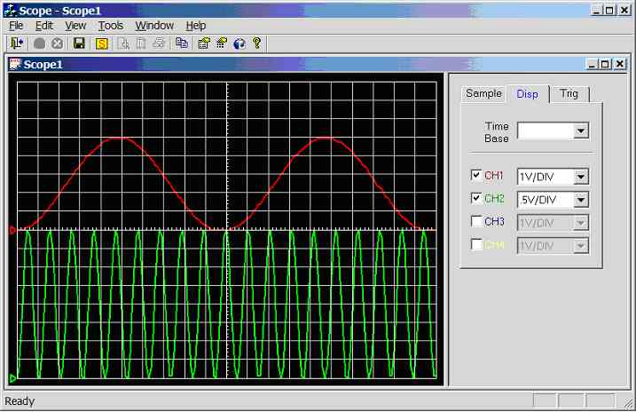 Figure 11.3.2.1h.
Screen dump of scope program (sample rate = 1 kHz, CH1 = 10Hz sinewave, CH2 =
100Hz sinewave)
Channel 1
connected to 10Hz sine-wave (5Vpp), channel 2
connected to 100Hz sine-wave (4Vpp), see figure 11.3.2.1h.
Channel 1: unaffected.
Channel 2: 2 divisions per cycle, hence the
calculated frequency is 1/(1*0.01) = 100 Hz.
Figure 11.3.2.1h.
Screen dump of scope program (sample rate = 1 kHz, CH1 = 10Hz sinewave, CH2 =
100Hz sinewave)
Channel 1
connected to 10Hz sine-wave (5Vpp), channel 2
connected to 100Hz sine-wave (4Vpp), see figure 11.3.2.1h.
Channel 1: unaffected.
Channel 2: 2 divisions per cycle, hence the
calculated frequency is 1/(1*0.01) = 100 Hz.
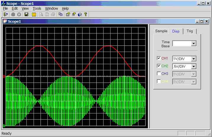 Figure 11.3.2.1i.
Screen dump of scope program (sample rate = 1 kHz, CH1 = 10Hz sinewave, CH2 =
550Hz sinewave)
Channel 1
connected to 10Hz sine-wave (5Vpp), channel 2
connected to 550Hz sine-wave (4Vpp), see figure 11.3.2.1i.
Channel 1: unaffected. Channel 2:
Under sampled, aliasing has occurred.
Figure 11.3.2.1i.
Screen dump of scope program (sample rate = 1 kHz, CH1 = 10Hz sinewave, CH2 =
550Hz sinewave)
Channel 1
connected to 10Hz sine-wave (5Vpp), channel 2
connected to 550Hz sine-wave (4Vpp), see figure 11.3.2.1i.
Channel 1: unaffected. Channel 2:
Under sampled, aliasing has occurred.
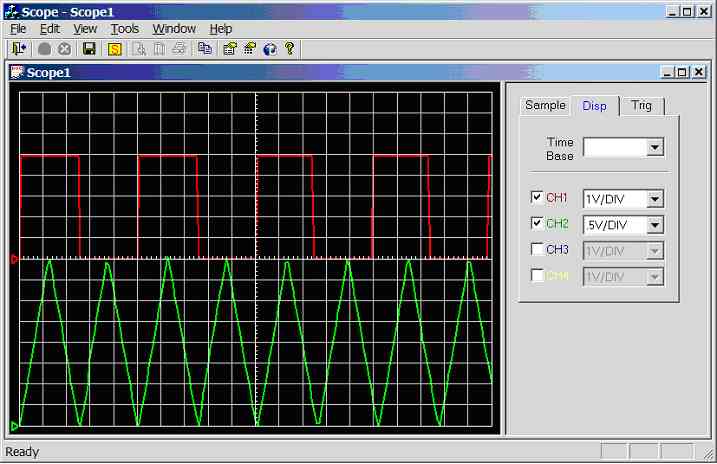 Figure 11.3.2.1j.
Screen dump of scope program (sample rate = 1 kHz, CH1 = square wave, CH2 =
trianglewave)
Note
all of the experiments (in this section) were carried using independent
triggering mode, because it was difficult to get two stable traces when
triggering off one channel (e.g. if triggering on CH1, CH2 is unstable, and if
triggering on CH2, CH1 was unstable). This problem should be software fixable.
11.3.2.2. Quad Channel Operation
Figure 11.3.2.1j.
Screen dump of scope program (sample rate = 1 kHz, CH1 = square wave, CH2 =
trianglewave)
Note
all of the experiments (in this section) were carried using independent
triggering mode, because it was difficult to get two stable traces when
triggering off one channel (e.g. if triggering on CH1, CH2 is unstable, and if
triggering on CH2, CH1 was unstable). This problem should be software fixable.
11.3.2.2. Quad Channel Operation
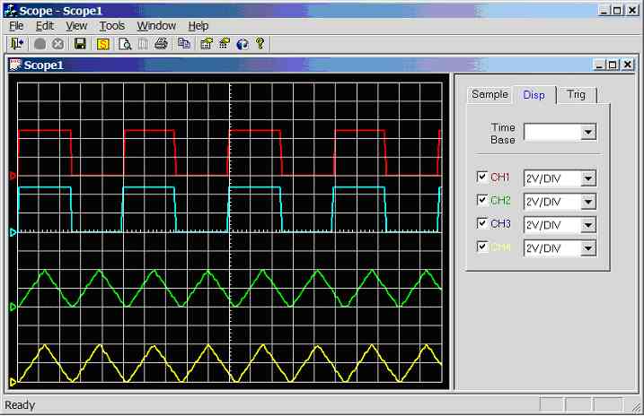 Figure 11.3.2.2a.
Screen dump of scope program (CH1 = CH2 = squarewave, CH3 = CH4 =
trianglewave)
Figure 11.3.2.2a.
Screen dump of scope program (CH1 = CH2 = squarewave, CH3 = CH4 =
trianglewave)
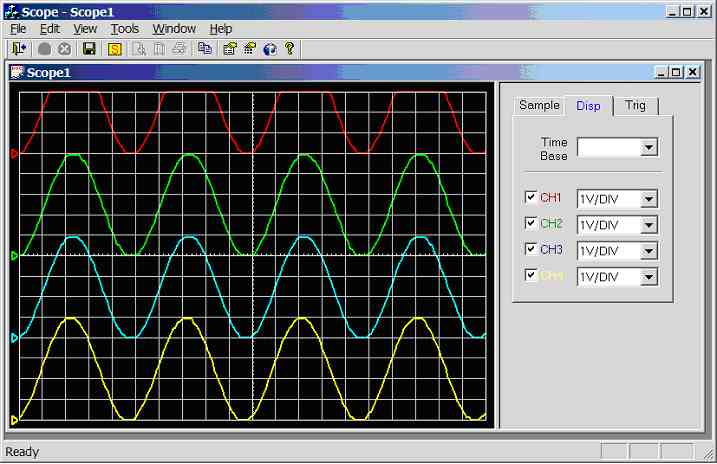 Figure 11.3.2.2b.
Screen dump of scope program (CH1 = CH2 = CH3 = CH4 = sinewave, triggering on
CH1)
All
waveforms in figure 11.3.2.2b were stable, note that there should be a 20µS
delay (see mark9.c) between each waveform (e.g. chop mode). For example
channel 1 should lead channel 2 by 20µS,
channel 2 should lead
channel 3 by 20µS etc… Each square represents
0.01 seconds (10mS); hence this small offset is not noticeable at this
resolution.
11.3.2.3. 5000Hz Sample Rate – Single Channel
mark9.c modified, basically the sample rate has been changed to 5000Hz (TimeBaseMUX
= 10), and sampling of channels 2 to 4 has been removed.
Note:
Sample rate = 5000Hz, 10
horizontal, samples per division. Hence scope time-base is 2 milliseconds per
division. Time-base is fixed on this version of the scope program.
50Hz
sinewave (0-5V) connected to CH1 (AN0), see figure 11.3.2.3a. 10 divisions per
cycle, hence the calculated frequency is 1/(10*0.002) = 50Hz.
Figure 11.3.2.2b.
Screen dump of scope program (CH1 = CH2 = CH3 = CH4 = sinewave, triggering on
CH1)
All
waveforms in figure 11.3.2.2b were stable, note that there should be a 20µS
delay (see mark9.c) between each waveform (e.g. chop mode). For example
channel 1 should lead channel 2 by 20µS,
channel 2 should lead
channel 3 by 20µS etc… Each square represents
0.01 seconds (10mS); hence this small offset is not noticeable at this
resolution.
11.3.2.3. 5000Hz Sample Rate – Single Channel
mark9.c modified, basically the sample rate has been changed to 5000Hz (TimeBaseMUX
= 10), and sampling of channels 2 to 4 has been removed.
Note:
Sample rate = 5000Hz, 10
horizontal, samples per division. Hence scope time-base is 2 milliseconds per
division. Time-base is fixed on this version of the scope program.
50Hz
sinewave (0-5V) connected to CH1 (AN0), see figure 11.3.2.3a. 10 divisions per
cycle, hence the calculated frequency is 1/(10*0.002) = 50Hz.
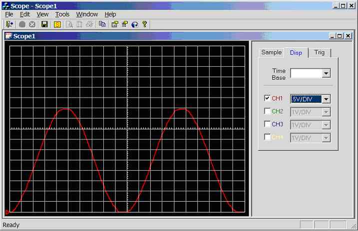 Figure 11.3.2.3a.
Screen dump of scope program (sample rate = 5000Hz, input wave = 50Hz sinewave
0-5V)
100Hz
sinewave (0-5V) connected to CH1 (AN0), see figure 11.3.2.3b. 5 divisions per
cycle, hence the calculated frequency is 1/(5*0.002) = 100Hz.
Figure 11.3.2.3a.
Screen dump of scope program (sample rate = 5000Hz, input wave = 50Hz sinewave
0-5V)
100Hz
sinewave (0-5V) connected to CH1 (AN0), see figure 11.3.2.3b. 5 divisions per
cycle, hence the calculated frequency is 1/(5*0.002) = 100Hz.
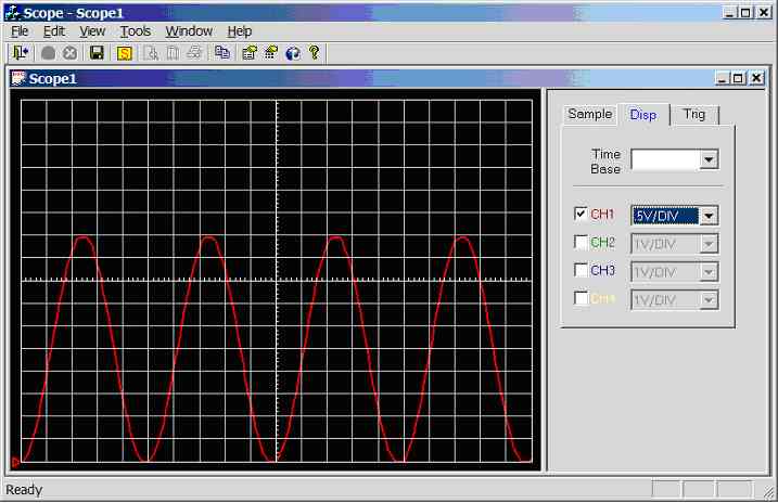 Figure 11.3.2.3b.
Screen dump of scope program (sample rate = 5000Hz, input wave = 100Hz
sinewave 0-5V)
200Hz
sinewave (0-5V) connected to CH1 (AN0), see figure 11.3.2.3c. 2.5 divisions
per cycle, hence the calculated frequency is 1/(2.5*0.002) = 200Hz.
Figure 11.3.2.3b.
Screen dump of scope program (sample rate = 5000Hz, input wave = 100Hz
sinewave 0-5V)
200Hz
sinewave (0-5V) connected to CH1 (AN0), see figure 11.3.2.3c. 2.5 divisions
per cycle, hence the calculated frequency is 1/(2.5*0.002) = 200Hz.
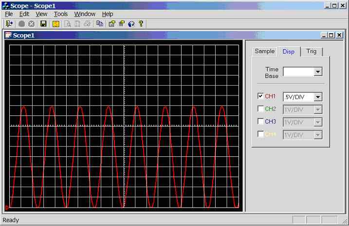 Figure 11.3.2.3c.
Screen dump of scope program (sample rate = 5000Hz, input wave = 200Hz
sinewave 0-5V)
300Hz
sinewave (0-5V) connected to CH1 (AN0), see figure 11.3.2.3d. 1.7 divisions
per cycle, hence the calculated frequency is 1/(1.7*0.002) = 294.1Hz.
Figure 11.3.2.3c.
Screen dump of scope program (sample rate = 5000Hz, input wave = 200Hz
sinewave 0-5V)
300Hz
sinewave (0-5V) connected to CH1 (AN0), see figure 11.3.2.3d. 1.7 divisions
per cycle, hence the calculated frequency is 1/(1.7*0.002) = 294.1Hz.
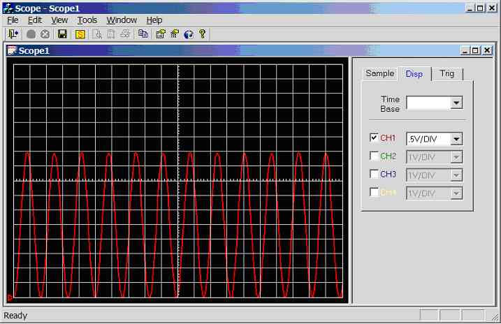 Figure 11.3.2.3d.
Screen dump of scope program (sample rate = 5000Hz, input wave = 300Hz
sinewave 0-5V)
400Hz
sinewave (0-5V) connected to CH1 (AN0), see figure 11.3.2.3e. 1.3 divisions
per cycle, hence the calculated frequency is 1/(1.3 *0.002) = 384.6Hz.
Figure 11.3.2.3d.
Screen dump of scope program (sample rate = 5000Hz, input wave = 300Hz
sinewave 0-5V)
400Hz
sinewave (0-5V) connected to CH1 (AN0), see figure 11.3.2.3e. 1.3 divisions
per cycle, hence the calculated frequency is 1/(1.3 *0.002) = 384.6Hz.
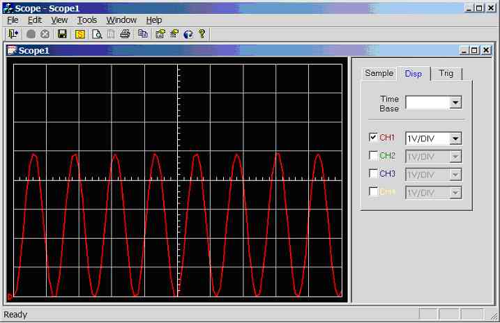 Figure 11.3.2.3e.
Screen dump of scope program (sample rate = 5000Hz, input wave = 400Hz
sinewave 0-5V)
500Hz
sinewave (0-5V) connected to CH1 (AN0), see figure 11.3.2.3f. 1 divisions per
cycle, hence the calculated frequency is 1/(1 *0.002) = 500Hz.
Figure 11.3.2.3e.
Screen dump of scope program (sample rate = 5000Hz, input wave = 400Hz
sinewave 0-5V)
500Hz
sinewave (0-5V) connected to CH1 (AN0), see figure 11.3.2.3f. 1 divisions per
cycle, hence the calculated frequency is 1/(1 *0.002) = 500Hz.
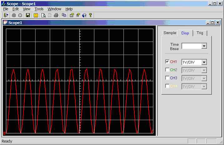 Figure 11.3.2.3f.
Screen dump of scope program (sample rate = 5000Hz, input wave = 500Hz
sinewave 0-5V)
750Hz
sinewave (0-5V) connected to CH1 (AN0), see figure 11.3.2.3g. 0.7 divisions
per cycle, hence the calculated frequency is 1/(0.7 *0.002) = 714.2Hz.
Figure 11.3.2.3f.
Screen dump of scope program (sample rate = 5000Hz, input wave = 500Hz
sinewave 0-5V)
750Hz
sinewave (0-5V) connected to CH1 (AN0), see figure 11.3.2.3g. 0.7 divisions
per cycle, hence the calculated frequency is 1/(0.7 *0.002) = 714.2Hz.
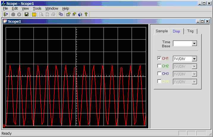 Figure 11.3.2.3g.
Screen dump of scope program (sample rate = 5000Hz, input wave = 750Hz
sinewave 0-5V)
1000Hz
sinewave (0-5V) connected to CH1 (AN0), see figure 11.3.2.3h. 0.5 divisions
per cycle, hence the calculated frequency is 1/(0.5 *0.002) = 1000Hz, but
distorted due to under sampling.
Figure 11.3.2.3g.
Screen dump of scope program (sample rate = 5000Hz, input wave = 750Hz
sinewave 0-5V)
1000Hz
sinewave (0-5V) connected to CH1 (AN0), see figure 11.3.2.3h. 0.5 divisions
per cycle, hence the calculated frequency is 1/(0.5 *0.002) = 1000Hz, but
distorted due to under sampling.
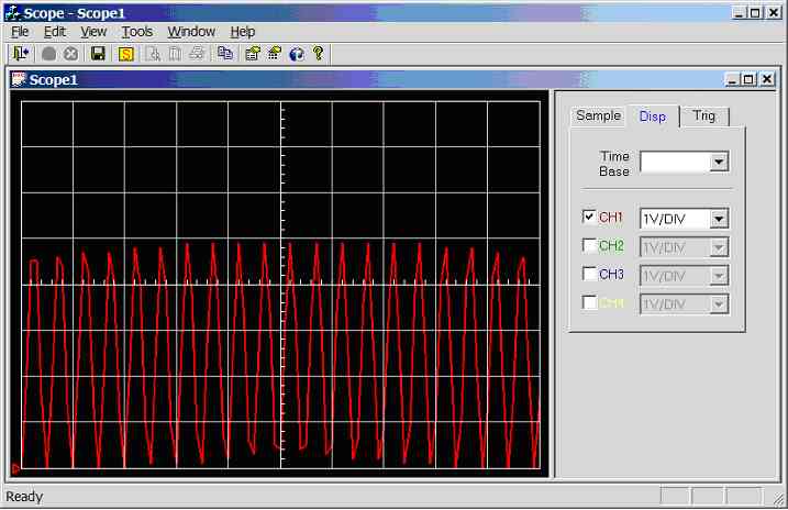 Figure 11.3.2.3h.
Screen dump of scope program (sample rate = 5000Hz, input wave = 1,000Hz
sinewave 0-5V)
2500Hz
sinewave (0-5V) connected to CH1 (AN0), see figure 11.3.2.3i. Under sampled.
Figure 11.3.2.3h.
Screen dump of scope program (sample rate = 5000Hz, input wave = 1,000Hz
sinewave 0-5V)
2500Hz
sinewave (0-5V) connected to CH1 (AN0), see figure 11.3.2.3i. Under sampled.
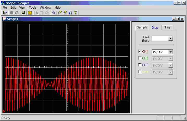 Figure 11.3.2.3i.
Screen dump of scope program (sample rate = 5000Hz, input wave = 2,500Hz
sinewave 0-5V)
Figure 11.3.2.3i.
Screen dump of scope program (sample rate = 5000Hz, input wave = 2,500Hz
sinewave 0-5V)
|
RX Terminal
-----------
Waiting for message (press a key to stop)
TEST RAM CHIP...
Test 1 - Fill RAM with 0xFF ---> Passes = 7806, Fails = 386
Test 2 - Fill RAM with 0x00 ---> Passes = 8114, Fails = 78
Test 3 - Fill RAM with LSB of Address ---> Passes = 31, Fails = 8161
End of RAMTEST, Hopefully work can now start on storage mode
|
This Web Page was last updated on Friday June 28, 2002
Home About me National Record Of Achievement Hobbies / Interests Guest Book Contact Me Links Snooker Amateur Radio Site Map
|
© 2002 Designed by Colin K McCord |
|
This website is best viewed by Microsoft Internet Explorer 6.0 at a resolution of 1024 x 768