|
|
|
|
3.0. Fundamentals |
|
|
|
|
|
3.0. Fundamentals |
|
3.1. The Basic CRT Oscilloscope
3.2. Digital
Sampling Oscilloscopes
3.3. Display
Formats
3.4. Aliasing
3.4.1. Typical Low-Pass
Filter Design Parameters
3.4.2. Typical Low-Pass Filter
3.4.3. Software Generation of an
Anti-Aliasing Filter
3.5. The PIC
Microcontroller
3.6. RS232
Serial Interface
3.1. The Basic CRT Oscilloscope
An oscilloscope draws its trace with a spot of light (produced by a deflectable beam of electrons) moving across the screen of its CRT (see Figure 1.0c). Basically an oscilloscope consists of the CRT, a ‘time base’ circuit to move the spot steadily from left to right across the screen at the appropriate time and speed, and some means (usually a ‘Y’ deflection amplifier) of enabling the signal to deflect the spot in the vertical or Y direction.
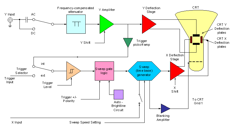
Figure 3.1a.
Block diagram of a basic CRT oscilloscope
This type of oscilloscope is known as a ‘real-time’ oscilloscope. This means that the vertical deflection of the spot on the screen at any instant is determined by the Y input voltage at that instant. Not all CRT oscilloscope are real-time instruments, figure 3.1b categorises the various types available.
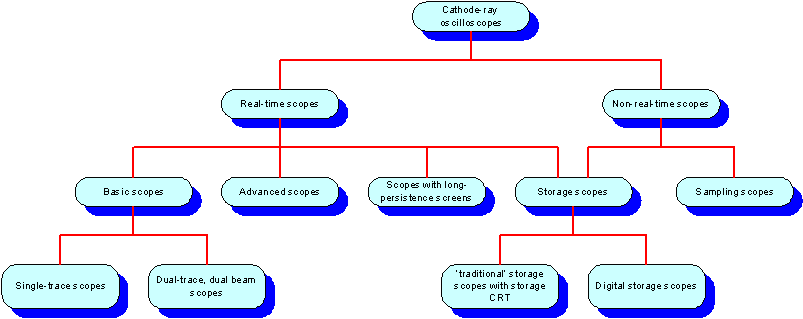
Figure 3.1b. Types of CRT oscilloscopes
3.2. Digital Sampling Oscilloscopes
Digital sampling oscilloscopes use an ADC (analogue-to-digital converter) to converter analogue voltages to binary representation. The sampling rate specifies the number of samples taken per second. Figure 3.2a demonstrates clearly how an analogue wave-form is digitally sampled and displayed onto the screen (LCD, Computer Monitor, etc…).
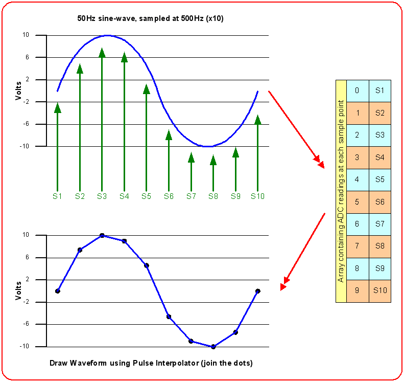
Figure 3.2a. Example showing how a sine-wave is digitally sampled
There are three main methods of presenting the captured waveform on the screen. These are dot display, dot joining (also called linear or pulse interpolation) and sine interpolation. These are illustrated in Figure 3.3a.
Dot display requires 20 to 25 samples per cycle before a recognisable sine wave can be plotted. Pulse interpolation provides a good general purpose display, where the waveform under investigation is known to be smooth and generally of a sinusoidal shape. Sine interpolation provides a good representation with as few as 2.5 samples per cycle. However, it should not in general be used for pulse waveforms, as here it can introduce ringing on the display which is not present on the actual waveform.
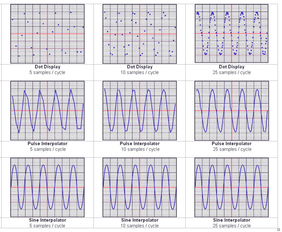
Figure 3.3a.
Comparison of Dot, Pulse Interpolator and Sine Interpolator displays at
different sample rates.
Nyquist theorem states that “to define a sine wave, a sampling system must take more than two samples per cycle”. Notice that the sine interpolator display type (2.5 samples / cycle) approaches the limits that the sampling theory suggests.
Exactly two samples per cycle (known as the ‘Nyquist rate’) suffice if it is guaranteed that they coincide with the peaks of the waveform. Otherwise there would be no knowledge of amplitude and if samples happened at zero crossings, the waveform wouldn’t even be detected. However more than two samples per cycle would be fine as the position of the samples relative to the sine wave will gradually drift through all possible phases, so that the peak amplitude will be accurately defined.
For none-sinusoidal waveforms, a sine interpolator is inappropriate, except in the case of certain instruments which can suitably pre-process the waveform before passing it to the sine interpolator.
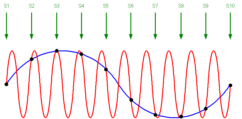
Aliasing is an undesirable effect that can occur in digital sampling oscilloscopes which is not found in traditional analogue oscilloscopes. This is the display of an apparent signal which does not actually exist, usually caused by under-sampling.
Many samples should be taken per cycle (at least 10 for pulse interpolation) to ensure an accurate representation of an analogue signal in a digital memory. If only one sample is taken per cycle, or one sample per several cycles, then aliasing occurs. For example say a waveform is being sampled every three cycles, these samples may form together, particularly when using pulse interpolation, to look like a valid waveform.
|
|
Figure 3.4a.
Demonstrating aliasing, red
is the real waveform, while blue is an alias.
Figure 3.4a clearly demonstrates how false signals (aliasing) can be displayed on a digital scope. The red waveform is the waveform being monitored, notice that the waveform is under sampled (see green arrows for sample points). The black dots shows were the input waveform (red) has been sampled, by joining the dots, it is clear that a perfect sine-wave is created (blue), which is an alias of the original signal. Note that it is impossible to tell that the blue signal is an alias, unless the scope has analogue and digital capabilities were a user can switch to analogue mode to check that the waveform is not an alias.
There is nothing that can be done after sampling to correct aliasing; hence the solution is to filter out high frequencies by sending the input signal through a low-pass filter. Ideally all frequencies above half the sample rate should be filtered out, but circuit design can become difficult if the sampling rate is adjustable because the high frequency cut-off must also be adjustable. One solution is to used digital potentiometers (resistance controlled by microcontroller), to change the high frequency cut-off of the filter.
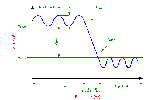
3.4.1. Typical Low-Pass Filter Design Parameters
There are four key parameters, that specify an low-pass filter as shown in figure 3.4.1a: fCUT-OFF, fSTOP, AMAX, and M.
|
Figure 3.4.1a. The key low pass filter design parameters |
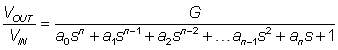
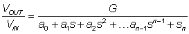
The cut-off frequency (fCUT-OFF) of a low pass filter is normally defined as the -3dB point (e.g. Butterworth and Bessel filter) or the frequency at which the filter response leaves the error band (e.g. Chebyshev).
Butterworth or Bessel filters do not create ripple in the pass band (i.e. flat) unlike the Chebyshev filter. The Chebyshev filter has a ripple up to the cut-off frequency, defined as ε.
“By definition, a low pass filter passes lower frequencies up to the cut-off frequency and attenuates the higher frequencies that are above the cut-off frequency.” [J4]
The filter order is determined by the number of poles in the transfer function (e.g. 3 poles, hence 3rd order). Generally, the greater number of poles a filter has the smaller the transition bandwidth.
“Ideally, a low-pass, anti-aliasing filter should perform with a ‘brick wall’ style or response, where the transition band is designed to be as small as possible. Practically speaking, this may not be the best approach for an anti-aliasing solution. With active filter design every two poles require an operational amplifier. For instance, if a 32nd order filter is designed, 16 operational amplifiers, 32 capacitors and up to 64 resistors would be required to implement the circuit. Additionally, each amplifier would contribute offset and noise errors into the pass band region of the response.” [J4]
3.4.2. Typical Low-Pass Filters
The Butterworth, Bessel, and Chebyshev are the three most popular filter designs, other filter types include: inverse Chebyshev, Elliptic and Cauer designs. See reference [B4] for detailed information on designing various types of filters including Butterworth and Chebyshev.
Butterworth Filter
The Butterworth filter is by far the most popular design used in circuits. This filter exhibits a monotonically decreasing transmission with all the transmission zeros at ω = ∞, making it an all-pole filter. Therefore the transfer function of a Butterworth filter consists of all poles and no zeros and is equated to: -
 {3.4.2.1}
Note denominator coefficients for Butterworth designs are available in table form; Table 1 in reference [J4] lists all of coefficient up to a 5th order filter. The frequency behaviour has a maximally flat magnitude response in the pass-band. The rate of attenuation in the transition band is better than Bessel, but not as good as the Chebyshev filter. There is no ringing in the stop band, but there is some overshoot and ringing in the time domain, but less than the Chebyshev.
Chebyshev Filter
“The Chebyshev filter exhibits an equiripple response in the pass-and and a monotonically decreasing transmission in the stop-and. While the odd-order filter has |T(0)| = 1, the even-order filter exhibits its maximum magnitude deviation at ω = 0. In both cases the total number of pass-and maxima and minima equals the order of the filter, N. All transmission zeros of the Chebyshev filter are at ω = ∞, making it an all-pole filter.” [B4]
Therefore the transfer function of the Chebyshev filter is similar to the Butterworth filter in that it has all poles and no zeros with a transfer function of: -
 {3.4.2.2}
Note denominator coefficients for Chebyshev designs are also available in table form; Table 2 in reference [J4] lists all of coefficient up to a 5th order filter.
Bessel Filter
The transfer function of the Bessel filter has only poles and no zeros. Where the Butterworth design is optimised for a maximally flat pass band response the transition bandwidth, the Bessel filter produces a constant time delay with respect to frequency over a large range of frequency. The transfer function for the Bessel filter is: -
 {3.4.2.3}
Note denominator coefficients for Bessel designs are also available in table form; Table 3 in reference [J4] lists all of coefficient up to a 5th order filter. The Bessel filter has a flat magnitude response in the pass-band, and the rate of attenuation in the transition band is slower than the Chebyshev or Butterworth. This filter has the best step response of all the filters mentioned, with very little overshoot or ringing.
3.4.3. Software Generation of an Anti-Aliasing Filter
Customised filters (e.g. anti-aliasing) can be designed automatically using powerful software applications, microchip have developed a program called ‘FillerLab’. This program is freeware and can be downloaded free of charge from the microchip website [W3].
“FilterLab™ is an innovative software tool that simplifies active filter design. Available at no cost, the FilterLab active filter software design tool provides full schematic diagrams of the filter circuit with component values and displays the frequency response.
FilterLab™ allows the design of low-pass filters up to an 8th order filter with Chebyshev, Bessel or Butterworth responses from frequencies of 0.1 Hz to 10 MHz. Users can select a flat passband or sharp transition from passband to stopband. Options, such as minimum ripple factor, sharp transition and linear phase delay, are available. Once the filter response has been identified, FilterLab™ generates the frequency response and the circuit. For maximum design flexibility, changes in capacitor values can be implemented to fit the demands of the application. FilterLab™ will recalculate all values to meet the desired response, allowing real-world values to be substituted or changed as part of the design process.
Further consideration is given to designs used in conjunction with an
analogue-to-digital converter. A suggested filter can be generated by simply
input-ting the bit resolution and sample rate via the Anti-Aliasing Wizard. This
eliminates erroneous signals folded back into the digital data due to the
aliasing effect.”
[W3]
A PIC (Peripheral Interface Controller) microcontroller is an IC manufactured by Microchip.
|
|
|
These ICs are complete computers in a single package. The only external components necessary are whatever is required by the I/O devices that are connected to the PIC.
The traditional Von-Neumann Architecture (Used in: 80X86, 8051, 6800, 68000, etc…) is illustrated in Figure 3.5a. Data and program memory share the same memory and must be the same width.
“All the elements of the von Neumann computer are wired together with the one common data highway or bus. With the CPU acting as the master controller, all information flow is back and forward along these shared wires. Although this is efficient, it does mean that only one thing can happen at any time. This phenomenon is sometimes known as the von Neumann bottleneck.” [B3]
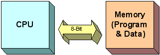
Figure 3.5a. Simplified illustration of the von Neumann architecture
PICs use the Harvard architecture. The Harvard architecture (Figure 3.5b) is an adaptation of the standard von Neumann structure with separate program and data memory: data memory is made up by a small number of 8-bit registers and program memory is 12 to 16-bits wide EPROM, FLASH or ROM.
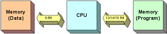
Figure 3.5b. Simplified illustration of the Harvard architecture
Traditional CISC (Complex Instruction Set Computer) machines (Used in: 80X86, 8051, 6800, 68000, etc…) have many instructions (usually > 100), many addressing modes and it usually takes more than 1 internal clock cycle to execute. PIC microcontrollers are RISC (Reduced Instruction Set Computer) machines, which have 33 (12-bit) to 58 (15-bit) instructions, reduced addressing modes (PICs have only direct and indirect), each instruction does less, but usually executes in one internal clock.
“The combination of single-word instructions, the simplified instruction decoder implicit with the RISC paradigm and the Harvard separate program and data buses gives a fast, efficient and cost effective processor implementation.” [B3]
3.5.1. Summary of the PICs Built-in Peripherals
SPI (Serial Peripheral Interface) uses 3 wires (data in, data out, clock), Master/Slave (can have multiple masters), very high speed (1.6 Mbps), and full speed simultaneous send and receive (full duplex).
I2C (Inter IC) uses 2 wires (data and clock), Master/Slave. There are lots of cheap I2C chips available; typically < 100kbps.
UART (Universal Asynchronous Receiver/Transmitter) with baud rates of 300bps to 115kbps, 8 or 9 bits, parity, start and stop bits, etc. Outputs 5V hence an RS232 level converter (e.g. MAX232) is required.
Timers, both 8 and 16 bits, many have prescalers and some have postscalers. In 14 bit cores they generate interrupts. External pins (clock in/clock out) can be used for counting events.
Ports have two control registers: TRIS sets whether each pin is an input or an output and PORT sets their output bit levels. Note: Other peripherals may steal pins, so in this respect peripheral registers control ports as well. Most pints have 25mA source/sink (LED enabled), but not all pins, it is important to look up the datasheet. Floating input pints must be tied off (or set to outputs).
ADCs (Analogue to Digital Converter) are currently slow, less than 54 KHz sampling rate (8, 10 or 12 bits), theoretically higher accuracy when PIC is in sleep mode (less digital noise) once the sample is complete the ADC sends an interrupt waking the PIC. Note that the PIC must wait until the sampling capacitor is charged; see datasheets.
RS232 is simple, universal, well understood and supported, but it has some serious shortcomings as a data interface. Its origins predate modern computers and it contains many features that are not relevant to the modern user. It can control very old primitive modems and has many control signals to do this in hardware, but often it is used without these old control and status lines.
Its major feature is that it does not require the transmission of a clock, the reception of a ‘start bit’ is enough to cause the receiver to time all its actions from this one edge. This is called asynchronous transmission. RS232 allows a 5% difference in transmitted timings and receiver chip timings. This is important if using a PIC as the datasheet specifies the % error of the baud rate generator at certain baud rates (the higher the baud rate, the higher the % error), as long as this error is less than 5% the RS232 standard is capable of coping.
Electronic data communications between elements will generally fall into two broad categories: single-ended and differential. RS232 (single-ended) was introduced in 1962, and despite rumours for its early demise, has remained widely used.
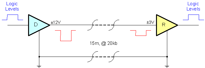
Figure 3.6a. Illustration of RS232, 1 driver and 1 receiver
“Both RS232 and RS423 are unbalanced (or single-ended) standards, where the receiver measures the potential between signal line and ground reference. Even though the transmitter and receiver grounds are usually connected though the transmission line return, the impedance over a long distance may support a significant difference in the two ground potentials, which will degrade noise immunity. Furthermore, any noise induced from the outside will affect signal lines differently from the ground return due to their dissimilar electrical characteristics – hence the name unbalanced.” [B3]
RS232 data is bi-polar, e.g. a +3 to +15 volt indicates an SPACE (ON) while a -3 to -15 volt indicates an MARK (OFF). Modern computer equipment ignores the negative level and accepts a zero voltage level as the MARK (OFF) state. This means circuits powered by 5 VDC are capable of driving RS232 circuits directly; however, the overall range that the RS232 signal may be transmitted / received is dramatically reduced.
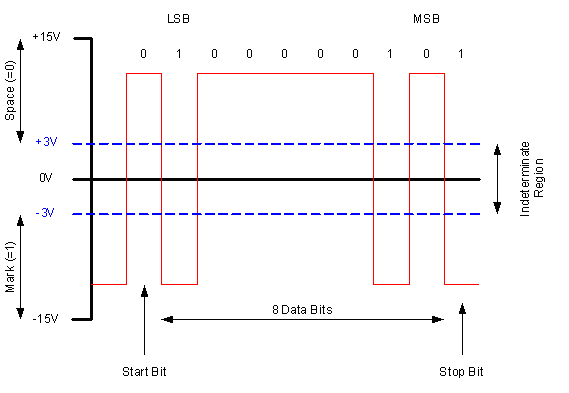
Figure 3.6d. Illustration of how data is transmitted over RS232
The output signal level usually swings between +15V and -15V. The ‘dead area’ between +3v and -3v is designed to give some noise immunity. This dead area can vary for various RS232 like definitions, for example the definition for V.10 has a noise margin from +0.3V to -0.3V. Many receivers designed for RS232 are sensitive to differentials of 1v or less.
|
|
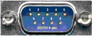
Pin |
Signal |
Pin |
Signal |
|
1 |
Data Carrier Detect |
6 |
Data Set Ready |
|
|
2 |
Receive Data |
7 |
Request to Send |
|
|
3 |
Transmit Data |
8 |
Clear to Send |
|
|
4 |
Data Terminal Ready |
9 |
Ring Indicator |
|
|
5 |
Signal Ground |
|
|
Figure 3.6b. 9-pin
RS232 D-connector, pin signal description
Typical line drivers / receivers chips for RS232 are the Maxim MAX232 or MAX233 chips (see http://www.maxim-ic.com) the original specification states that RS232 should drive 50 feet, but modern line driver/receivers can manage much better than this.
|
Baud Rate |
Max Distance Shielded Cable |
Max Distance Unshielded Cable |
|
110 bps |
5000 feet |
3000 feet |
|
300 bps |
5000 feet |
3000 feet |
|
1200 bps |
3000 feet |
3000 feet |
|
2400 bps |
1000 feet |
500 feet |
|
4800 bps |
1000 feet |
250 feet |
|
9600 bps |
250 feet |
250 feet |
Figure 3.6c. Typical maximum distance modern line driver/receivers can manage before errors occur.
This Web Page was last updated on Friday June 28, 2002
Home About me National Record Of Achievement Hobbies / Interests Guest Book Contact Me Links Snooker Amateur Radio Site Map
|
© 2002 Designed by Colin K McCord |
|
This website is best viewed by Microsoft Internet Explorer 6.0 at a resolution of 1024 x 768