|
|
|
|
4.0. The PIC16F877 Microcontroller |
|
|
|
|
|
4.0. The PIC16F877 Microcontroller |
|
4.0.
Architecture of the PIC16F877
microcontroller
4.1. Overview of
the File Registers
4.2. Overview of the 8-channel
10-bit ADC
4.3. Overview of
the Hardware USART
4.3.1 Baud-Rate Generator, BRG
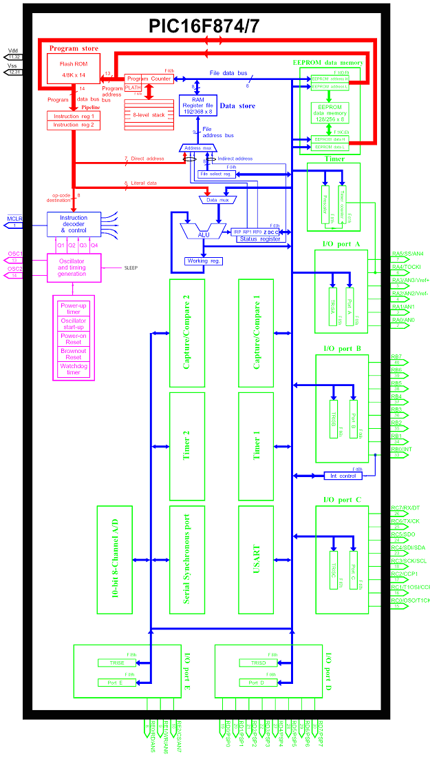
Figure 4.0a:
Architecture of the PIC16F877 microcontroller [W9]
“The PIC16F877 is a high-performance FLASH microcontroller that provides engineers with the highest design flexibility possible. In addition to 8192x14 words of FLASH program memory, 256 data memory bytes, and 368 bytes of user RAM, PIC16F877 also features an integrated 8-channel 10-bit Analogue-to-Digital converter. Peripherals include two 8-bit timers, one 16-bit timer, a Watchdog timer, Brown-Out-Reset (BOR), In-Circuit-Serial Programming™, RS-485 type UART for multi-drop data acquisition applications, and I2C™ or SPI™ communications capability for peripheral expansion. Precision timing interfaces are accommodated through two CCP modules and two PWM modules.” [W3]
4.1. Overview of the File Registers
The data memory is partitioned into multiple banks which contain the general purpose registers and the special function registers. Bits RP1 and RP0 are the bank select bits, these bits are found in the STATUS register (b6 & b5).
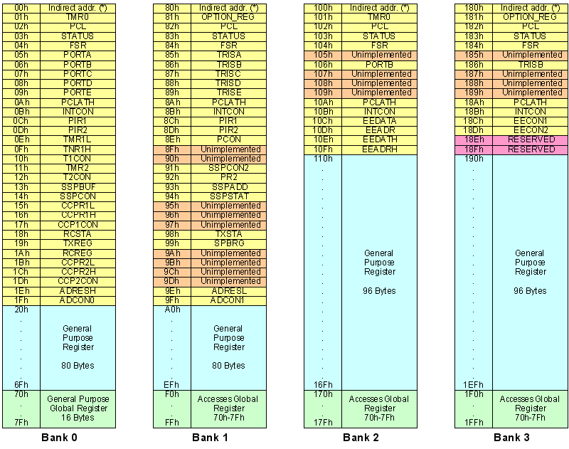
Figure 4.1a. PIC16F877 register file map
Each bank extends up to 7Fh (128 bytes). The lower locations of each bank are reserved for the special function registers (shown in yellow). Above the special function registers are general purpose registers (shown in blue), implemented as static RAM. All implemented banks contain special function registers. Some “high use” special function registers from one bank may be mirrored in another bank for code reduction and quicker access. Also notice that there are 16 general purpose global registers (shown in green), these registers can be accessed from any bank.
4.2. Overview of the 8-Channel 10-bit ADC
At first it appears that the PIC16F877 has 8 built-in ADCs, but this is not the case. Figure 4.2a shows a simplified block diagram of the analogue-to-digital converter module, clearly there is only one 10-bit ADC which can be connected to only one of eight input pins at any one time.
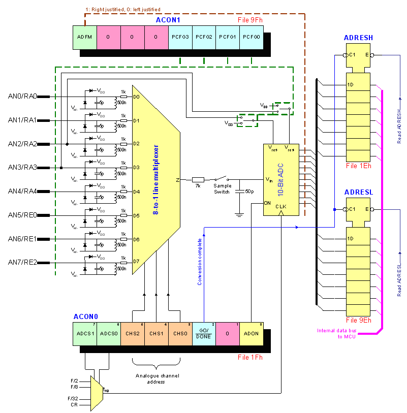
Figure 4.2a. Simplified block diagram of the PIC16F877 ADC module
The input analogue channels AN4..0 are shared with port A, and channels AN7..5 are shard with port E. If less than eight analogue channels are required then some of the pins can be assigned as digital I/O port lines using PCFG3..0 bits (see datasheet). For example, if PCFG3..0 = 0010 then AN4..0 are configured as analogue inputs, while AN7..5 are digital (port E free), with VDD used as the reference.
“On reset all pins are set to accept analogue signals. Pins that are reconfigured as digital I/O should never be connected to an analogue signal. Such voltage may bias the digital input buffer into its linear range and the resulting large current could cause irreversib
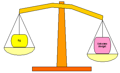
le damage.” [B3]The 10-bit ADC uses a technique know as ‘successive approximation’, the following mechanical analogy will help explain how it works. Suppose there is an unknown weight, a balance scale and a set of precision known weights 1, 2, 4 and 8 grams. A systemic technique can be used to calculate the unknown weight.
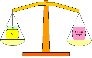
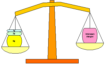
Place the 8g weight on the pan and remove if it is too heavy. Next place the 4g weight on the pan and remove if it is too heavy. Next place the 2g weight on the pan and remove if it is too heavy. Next place the 1g weight on the pan and remove if it is too heavy. The sum of the weights still on the pan yields the nearest lower value of the unknown weight. This is illustrated in figures 4.2b to 4.2g.
|
Figure 4.2b. Unknown weight placed on the scales |
Figure 4.2c. 8g weight placed on the pan, not too heavy (keep) |
|
Figure 4.2d. 4g weight placed on the pan, too heavy (remove) |
Figure 4.2e. 2g weight placed on the pan, not too heavy (keep) |
|
Figure 4.2f. 1g weight placed on the pan, too heavy (remove) |
Figure 4.2g. Unknown weight is about 10g (1010) |
The electronic equivalent to this successive approximation technique uses a network of precision capacitors configured to allow consecutive halving of a fixed voltage VREF to be switched in to an analogue comparator, which acts as the balance scale.
Generally the network of capacitors are valued in powers of two to subdivide the analogue reference voltage (e.g. 1,2,4,8,16, etc…). This sampling acquisition process takes a finite time due to the charging time constant and is specified in the datasheet as 19.72µS.
4.3. Overview of the Hardware USART
The Universal Synchronous Asynchronous Receiver Transmitter (USART) module is one of the two serial I/O modules. The USART can be configured for asynchronous operation (UART) for communication with a PC or synchronous operation for communicating with peripheral devices such as DAC or DAC integrated circuit.
Note bit SPEN (RCSTA:7) and bits TRISC:7..6 have to be set in order to configure pin PC6/TX/CK and RC7/RX/DT for USART operation. CSS (C compiler) will automatically configure these bits, but it is important to be aware that if using fast_io(C) mode to manually configure port C, bits 7 & 6 must also be manually set if using the hardware UART.
4.3.1. Baud-Rate Generator, BRG
This is basically a
programmable 8-bit counter followed by a switchable frequency
![]() flip flop chain which can be set up to give the appropriate
sampling and shifting rates for the desired baud rate, based on the PIC’s
crystal frequency XTAL (e.g. for 20MHz, XTAL = 20) giving: -
flip flop chain which can be set up to give the appropriate
sampling and shifting rates for the desired baud rate, based on the PIC’s
crystal frequency XTAL (e.g. for 20MHz, XTAL = 20) giving: -
![]()
![]() {4.3.1.2}
{4.3.1.2}
![]() {4.3.1.3}
{4.3.1.3}
It may be advantageous to use the high baud rate (BRGH = 1) even for slower baud clocks as this may reduce baud rate error in some cases.
This Web Page was last updated on Friday June 28, 2002
Home About me National Record Of Achievement Hobbies / Interests Guest Book Contact Me Links Snooker Amateur Radio Site Map
|
© 2002 Designed by Colin K McCord |
|
This website is best viewed by Microsoft Internet Explorer 6.0 at a resolution of 1024 x 768