|
|
|
|
5.0. Hardware Development |
|


5.1. Simplified Block Diagram
5.2. Digital
Circuit Diagram
5.3. Analogue
Circuit Diagram - Mark 1
5.4. Analogue
Circuit Diagram - Mark 2
5.5. System
Powering Circuit
6.6. Cost of
Components
The purpose of this project is to design, built and test a low-cost PC-based digital real-time / storage oscilloscope. The main reasoning behind hardware development was to keep the hardware cost to an absolute minimum.
It was decided to use the PIC16F877 (flash version), “The PIC16F877 is a high-performance FLASH microcontroller that provides engineers with the highest design flexibility possible. In addition to 8192x14 words of FLASH program memory, 256 data memory bytes, and 368 bytes of user RAM, PIC16F877 also features an integrated 8-channel 10-bit Analogue-to-Digital converter. Peripherals include two 8-bit timers, one 16-bit timer, a Watchdog timer, Brown-Out-Reset (BOR), In-Circuit-Serial Programming™, RS-485 type UART for multi-drop data acquisition applications, and I2C™ or SPI™ communications capability for peripheral expansion. Precision timing interfaces are accommodated through two CCP modules and two PWM modules.
The PIC16F877 also supports low voltage self-programming, allowing the user to program the device in-circuit at the user’s operating voltage. The in-circuit debugging feature allows the designer to “emulate” the PIC16F877 device without an in-circuit emulator (the MCU itself is the “emulator”). PIC16F877 applications range from body controllers, programmable machine controls, network maintenance, feature phones and field-upgradeable pointing devices. PIC16F877 has 33 I/O pins and is available in the following package options: 40 PDIP(P), 44 PLCC(L), 44 PQFP(PQ), and 44 TQFP(PT)” [W3].
Four of the PICs ADC pins are used for data acquisition, a MAX232 buffer is used to convert the TTL serial logic of the PICs UART to the correct RS232 format. Additionally an analogue circuit is required to make sure the input voltage to the PICs ADC falls between 0 to 5V, Figure 5.0a illustrates an -10 to 10V sine wave, where the 10V peak is reduced to 5V (ADC Value is 1024), 0V is represented by 2.5V (ADC Value is 512) and -10V is represented by 0V (ADC value is 0), i.e. Bipolar. This could be achieved using two 741 op-amps, and a couple of diodes could be used for protection as the ADC cannot handle voltages outside its range (damage the PIC).
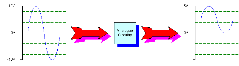
Figure 5.0a. Illustrates the operation of the analogue circuitry
A 5V voltage regulator (7805) is used to power the circuit; hence there is a large DC input range of 7 to 20V. This means that a standard DC power supply (7 to 20VDC) or a battery source (e.g. 9V PP3) can be used to power circuit.
Figure 5.1a, shows a simplified block diagram of the overall system. It is clear the PIC is connected to a MAX232 buffer which is connected to the PCs RS232 port. Notice that the clock is specified as 20MHz this was not the original plan, as a slower clock speed would reduce power consumption (critical if using battery power supply) and less noise would have been generate; hence ADC readings would be more accurate, allow it is possible to put the PIC to sleep while taking the ADC reading, the ADC will send an interrupt waking the PIC once the acquisition is complete. This is not an option for this application because it takes a long time for the PICs oscillator to return to full speed, after a sleep operation; hence this would severely affect the maximum sampling rate.
The main reason for using a 20MHz clock was because at slower clock speeds it was not possible to obtain a good 115kbps baud rate. Officially the maximum allowable baud rate error is 3%; allow most PC UARTs are specified to operate correctly with a baud rate variation of 5% before many errors start to occur. The C compiler (CCS V2.7) used to write the PIC program, generates an error if the specified baud rate cannot be achieved within 3% of the desired value using the current clock rate. The reason why 115kbps is important is because the RS232 serial communication is the bottleneck when operating in real-time mode; hence it makes sense to use the maximum baud rate possible. Note the PIC is capable at 20MHz of generating baud rates higher than 115kbps, but most PCs have a maximum baud rate of 115kbps.
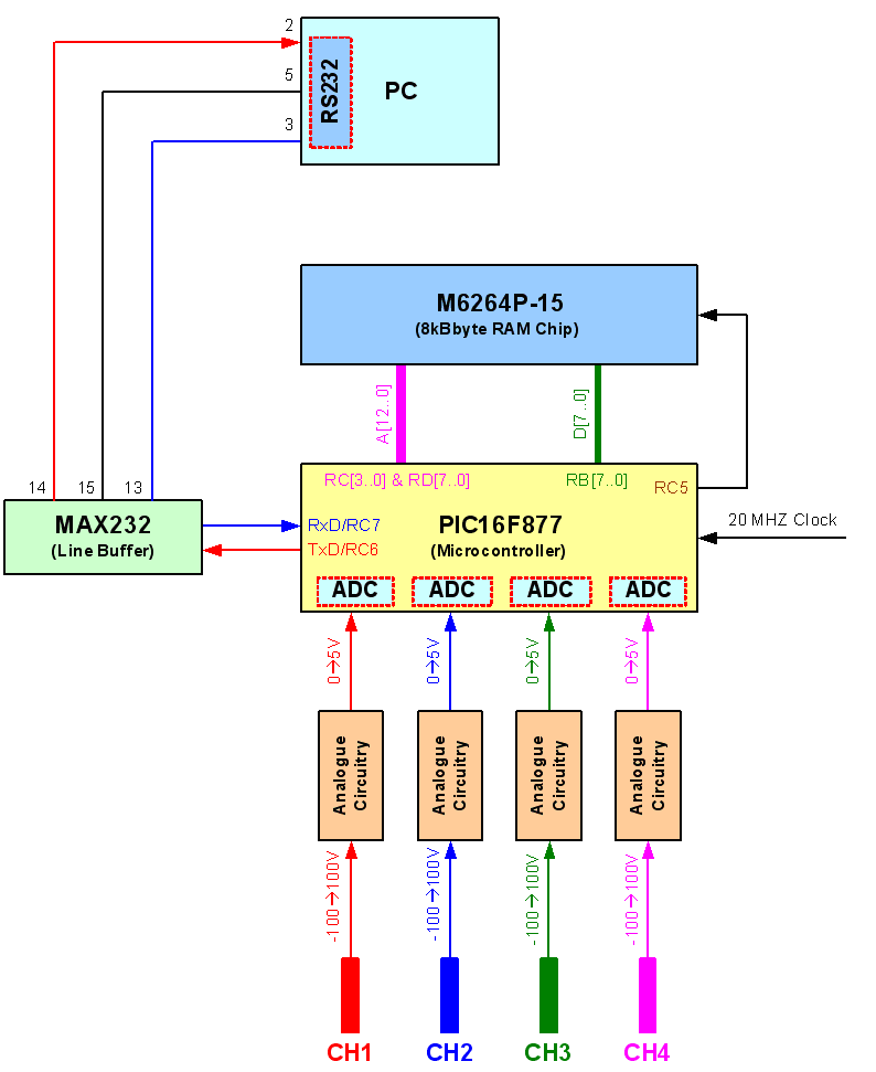
Figure 5.1a. Simplified Block diagram
The block diagram (figure 5.1a) clearly illustrates that the analogue circuitry required for each channel is identical. Note four 741 op-amps are available in a single IC chip, that’s two op-amp ICs required in total (2 741s for each analogue circuit block).
Not shown on this diagram (which is one option) is the input of additional control lines from the PIC to each “Analogue Circuitry” block. These control lines will be used to select different input voltage ranges, e.g. -1V to 1V, -10V to 10V, -100V to 100V. Analogue switches could be used to switch in different resistor values to the op-amps, hence changing the gain of the op-amp (MAX4066 or MM74HC4066). A better solution is the use of digital potentiometers (resistance controlled by microcontroller), to change the gain of the op-amp. At first it appears that there is not enough free pins on the PIC to control the analogue input range, this is true, but it is possible use the data and address bus as long as the RAM chip is disabled. But this mains that additional IC chips are required (latches, e.g. 74373 is an 8-bit parallel latch) to hold the selected range while the PIC is using these lines for use with the RAM chip.
The simplest way of producing different analogue ranges is to have a number of different inputs, for example each analogue block has 3 inputs: -1 to 1V, -10 to 10V and -250 to 250V. Another simple solution is to use a manual three-to-one way switch to select the appropriate range.
It is clear that a 8kByte RAM chip (see figure 5.1a) is used, this RAM chip is used during storage mode operation. A finite number of samples are stored into the RAM chip and transmitted to the PC in one large block, hence removing the RS232 bottleneck (faster sample rates possible). Notice that there are 8 data lines which are connected to port B and 13 address lines connected which are connected to port C and port D. Recall that 2 bytes are required per reading, hence 4000 readings can be stored, that’s 1000 for each channel. Notice that there is one control line: this puts the RAM chip in read or write mode, but if the data lines are shared with another component sometime in the future there is the need for another control line to disable the RAM chip.
It is possible to use four PICs (one for each channel) hence each channel can be sampled simultaneously, using a master/slave communication protocol. For example each PIC has its own address (say 1 to 4) all four wait until the master (PC) calls them before transmitting there data. Note: the current communication protocol would not work because there is a high likelihood of a collision occurring (two or more transmit at the same time), hence the need for a master/slave communication protocol or extremely good synchronisation where each PIC only transmits during specified time blocks. Sampling simultaneously is not required, the two modes chop and alt should be adequate, hence only one PIC is required (chop: read CH1 à read CH2 à read CH3 àread CH4 à ..., alt: read CH1 1000 times à read CH2 1000 times à read CH3 1000 times à read CH4 1000 times). Simultaneous sampling using four PICs may be useful for specialist applications and this project is suitable as only mirror software modification is required.
Figure 5.2a shows the digital circuit diagram, the design is simple with a low chip count (3 ICs).
|
S2 |
S1 |
S0 |
Baud Rate |
|
0 |
0 |
0 |
115,200 bps |
|
0 |
0 |
1 |
57,600 bps |
|
0 |
1 |
0 |
38,400 bps |
|
0 |
1 |
1 |
32,768 bps |
|
1 |
0 |
0 |
19,200 bps |
|
1 |
0 |
1 |
14,400 bps |
|
1 |
1 |
0 |
9,600 bps |
|
1 |
1 |
1 |
4,800 bps |
|
Figure 5.2b. Dip-switch configuration |
|||
The dip-switches connected to port E are used to select RS232 baud rate (see figure 5.2b). The MAX232CPE (RS232 line buffer) is connected to pins RC7 and RC6 of the PIC; these pins are for use with the PICs hardware UART. The use of the PICs hardware UART was the only option, because a software UART would severely affect system performance.
The reason why the MAX232CPE (RS232 line buffer) was chosen was because it can be powered from a single 5V power supply. Recall that RS232 requires +3 to +12 volts for a logic ‘0’ and -3 to -12 volts for a logic ‘1’, the MAX232CPE has a built-in (external capacitors required) voltage doubler circuit (+10V) and a voltage inverter circuit (-10V). This reduces product cost as the other option is to using a switch mode DC to DC converter (cost about £5) to generate required power supply. Allow a +15 and -15 supply is required for the analogue circuit; hence a DC to DC converter is required anyway. Allow the max232 data sheet states that the +10 and -10 voltage pins could be used to drive other circuits, but it is not recommended, plus its good design practice to keep analogue and digital circuits separate (problems with noise).
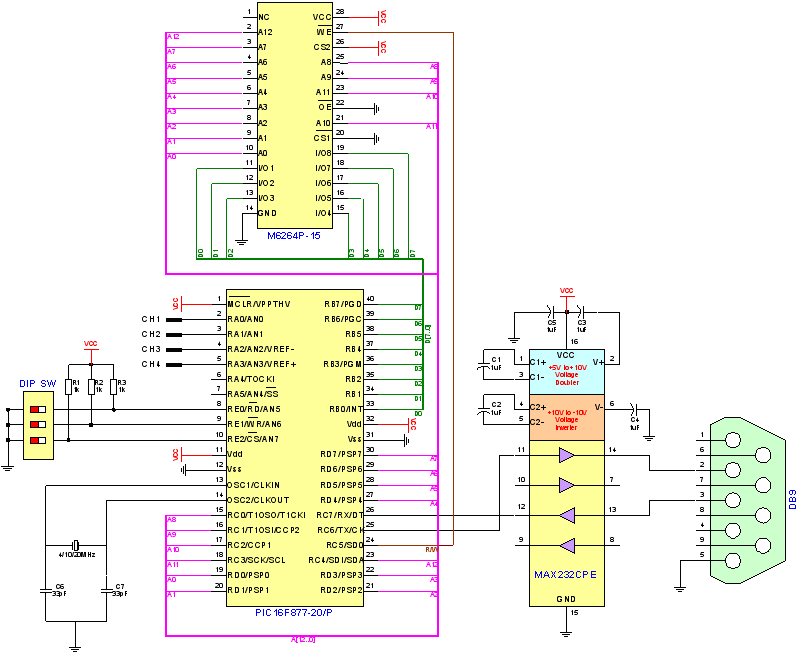
Figure 5.2a. Digital circuit diagram (version 1.3, 19/03/2002)
Port D is used for the first 8-bits of the 13-bit address bus (213 = 8192 address), RC4 to RC0 is used for the upper 5-bits of the address bus and Port B is used for the 8-bit data bus. The only component making use of the data and address buses is the external RAM chip, hence there is only the need for one control line (R/W), this control line (R/W) puts the RAM chip in read or write mode. If the data and buses are shared with other components sometime in the future the RAM chip must be disable, while communicating with these devices, this requires an additional control line (/OE).
To reduce cost even further a 28-pin version of the chosen PIC (PIC16F876) could be used, but this means a serial RAM chip must be used. The operation of a serial RAM chip is much slower than a parallel RAM chip, as each bit of the address and data must be clocked in one bit at a time. The purpose of the RAM chip is to compensate for the RS232 bottleneck (serial link); surly a serial RAM chip would have the same bottleneck. Yes it does, but the maximum baud rates are much faster than RS232, hence a serial RAM chip is a real possibility especially now the PIC is running at 20 MHz (must used 20MHz for high RS232 baud rate).
The ADC input channels (RA3..RA0) labelled CH4..CH1 are connected to the output of the analogue circuit.
5.3. Analogue Circuit Diagram - Mark 1
Figure 5.3a shows the circuit diagram for ensuring that the input voltage falls between zero and five volts. The first op-amp is designed to change the input voltage so that it does not go over 0 volts, for example changes -1 to 1V, to 0 to -2V. The second op-amp is configured in a negative amplifier mode to increase and change 0 to -2V, to 0 to 5V. Note the third part with the two zener diodes is for protection, the PIC ADCs may be damaged if input voltage is larger than 5 volts or smaller than 0 volts.
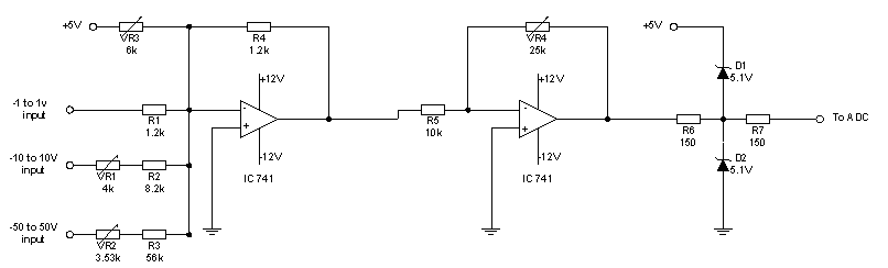
Figure 5.3a. Analogue circuit diagram – Mark 1 (14/12/2001)
The variable resistors are for calibration: -
1. Ground -1 to 1V input, calibrate using VR3 until -1.5V is outputted from the first op-amp.
2. Change VR4 until 2.5 volts is outputted from the output after the two zener diodes and the 2 150R resistors.
3. Un-ground -1 to 1v input and put in a voltage into input -10 to 10v and calibrate using VR1. Disconnect that voltage.
4. Put a voltage in to -50 to 50V and calibrate using VR2.
Disadvantages of this circuit: -
1. Use of variable resisters (much more expensive than fixed value resistors).
2. No op-amp protection if wrong input line is used (e.g. 100V input on the -1 to 1V input).
3. If an input line is used (say -10 to 10V line) and a device is connected to another line (e.g. say -1 to 1V line) there is nothing to stop current flow to the other device. A diode could be used but there is a 0.7 voltage drop across the diode, resistor values could be changed to compensate for this voltage drop.
4. Range not microcontroller controlled.
5.3.1 Simulation of the Circuit using Electronic Workbench
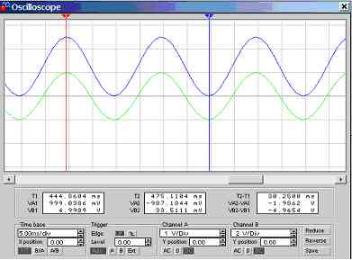
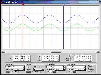
From figure 5.3.1a (using -1 to 1V input) it is clear that a -1 to 1V sine-wave input has been applied and the output is 0 to 5V. Figure 5.3.1b clearly shows an input of -0.5v to 0.5v, and an output of to 1.25V to 3.75V. Notice the input and output waveforms are the same phase and polarity.
|
Figure 5.3.1a. Screen dump of oscilloscope (CH A: Input, CH B: Output) |
Figure 5.3.1b. Screen dump of oscilloscope (CH A: Input, CH B: Output) |
5.4. Analogue Circuit Diagram - Mark 2
Figure 5.4a shows the modified circuit diagram for ensuring that the input voltage falls between zero and five volts, without the use of variable resistors. The first op-amp is designed to change the input voltage so that it does not go over zero volts, for example changes -2.5 to 2.5V, to -5 to 0V. The second op-amp is configured in negative amplifier mode with a gain of unity changing -5 to 0V to 0 to 5V. The third part with the two diodes is for protection, e.g. say a -1 to 6V signal makes it through the op-amps the diodes will cut off the peaks of the waveform making sure no damage is done to the PICs ADC. Note for the -250 to 250V range it may be necessary for R3 to be made up of several resistors in series as standard resisters have a maximum operating voltage of about 200 volts. All resistors should have a tolerance of at least 1%; ideally instrumental resistors should be used.
Instead of three inputs it is recommend that a three-to-one line manual switch should be used to connect each line to a single input line. Over voltage protection is still required in case of miss use, e.g. the user has the -2.5 to 2.5V volt input selected and connects the 240VAC mains to the input.
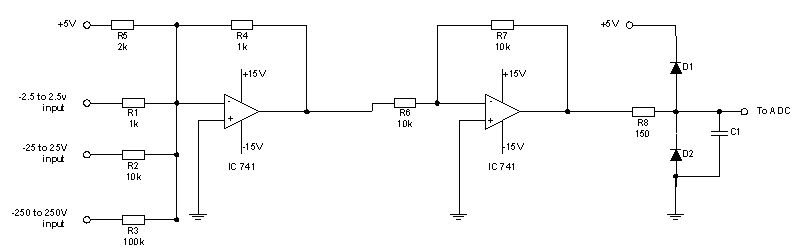
Figure 5.4a. Analogue circuit diagram – Mark 2 (19/03/2002)
Disadvantages of this circuit: -
1. No op-amp protection if wrong input line is used (e.g. 100V input on the -2.5 to 2.5V input).
2. Range not microcontroller controlled.
Figure 5.5a shows the circuit diagram; clearly a 5V regulator is used to generate a 5 volt DC output to power the circuit. The 0.1µF capacitors absorb line noise, while the 100µF capacitors are used for storage in the event of a minor drop in power (milliseconds) the circuit operation will not be affected.
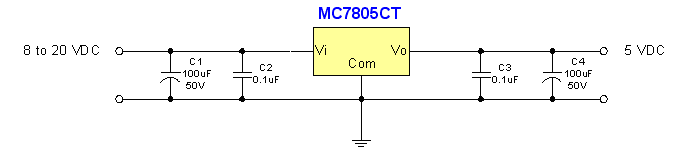
Figure 5.5a. System powering circuit
This means that the circuit has now got a wide operating voltage range as 8 to 20 volts DC will power the circuit. Note there are higher spec 7805 chips available that can operate up to 30 volts DC, if there is a need for a higher voltage range.
The system can be powered from a battery source (e.g. PP3 9V), or a DC power supply (e.g. 12V). It has been decided, not to design a complete power supply unit from scratch, but to use commercially available units. It is important to remember that voltage regulators are not efficient, and as the input voltage increases the least efficient they become, energy is lost in the form of heat. A heat sink is normally required to keep the chip within its maximum operational temperature.
All order numbers refer to Farnell catalogue.
Digital Circuit: -
|
Order Number |
Item |
Qty. |
Cost Each |
Cost |
|
325-5573 |
PIC16F877 – 20/P Microcontroller |
1 |
£7.09 |
£7.09 |
|
407-150 |
MAX232CPE – RS232 Line Buffer |
1 |
£2.40 |
£2.40 |
|
115-873 |
HT6264-70 (8k x 8) CMOS SRAM, 70ns acc |
1 |
£1.65 |
£1.65 |
|
170-234 |
20MHz Crystal A147C |
1 |
£0.75 |
£0.75 |
|
747-014 |
33pF Ceramic Capacitor |
2 |
£0.13 |
£0.26 |
|
664-315 |
1µF 25V Electrolytic Capacitor |
5 |
£0.27 |
£1.35 |
|
543-380 |
1kΩ Metal Oxide Film 1% Resistor |
3 |
£0.02 |
£0.06 |
|
134-3040 |
40-way dip docket |
1 |
£0.33 |
£0.33 |
|
134-3038 |
28-way dip socket |
1 |
£0.22 |
£0.22 |
|
134-2988 |
16-way dip socket |
1 |
£0.12 |
£0.12 |
|
780-091 |
4-way dip switch |
1 |
£0.40 |
£0.40 |
|
150-812 |
9-way D-type Socket |
1 |
£0.55 |
£0.55 |
|
|
|
|
Total |
£15.18 |
Analogue Circuit (Mark 2): -
|
Order Number |
Item |
Qty. |
Cost Each |
Cost |
|
300-373 |
Quad, 741 op-amp, LM348N |
2 |
£0.40 |
£0.80 |
|
134-2988 |
16-way dip socket |
2 |
£0.12 |
£0.12 |
|
543-380 |
1KΩ Metal Oxide Film 1% Resistor |
6 |
£0.02 |
£0.11 |
|
543-627 |
10KΩ Metal Oxide Film 1% Resistor |
9 |
£0.02 |
£0.17 |
|
543-457 |
2KΩ Metal Oxide Film 1% Resistor |
3 |
£0.02 |
£0.06 |
|
543-860 |
100KΩ Metal Oxide Film 1% Resistor |
3 |
£0.02 |
£0.06 |
|
543-860 |
150Ω Metal Oxide Film 1% Resistor |
3 |
£0.02 |
£0.06 |
|
352-5340 |
1N4007 Diode |
6 |
£0.04 |
£0.23 |
|
330-760 |
1W – DC to DC converter 5V input, -15, 15V output |
1 |
£5.05 |
£5.05 |
|
|
|
|
Total |
£6.66 |
System Powering Circuit: -
|
Order Number |
Item |
Qty. |
Cost Each |
Cost |
|
701-853 |
MC7805CT, 5V 1A Voltage Regulator |
1 |
£0.30 |
£0.30 |
|
920-757 |
100µF 50V Electrolytic Capacitor |
2 |
£0.10 |
£0.21 |
|
746-063 |
100pF Ceramic Capacitor |
2 |
£0.13 |
£0.26 |
|
178-701 |
Clip On Heat Sink |
1 |
£0.36 |
£0.36 |
|
|
|
|
Total |
£1.13 |
Total component cost = 15.18 + 6.66 + 1.13 = £22.97
This Web Page was last updated on Friday June 28, 2002
Home About me National Record Of Achievement Hobbies / Interests Guest Book Contact Me Links Snooker Amateur Radio Site Map
|
© 2002 Designed by Colin K McCord |
|