

Class A Amplifier Design - Part 1
|
|
|
|
Class A Amplifier Design - Part 1 |
|
Tip: print these pages out NOW! after loading.
This is quite a lengthy document and contains schematics as .gif files. Accordingly it may take some time to download - but well worth the wait. Please be patient.
These tutorials (parts 1 to part4) will teach you in very easy steps how to design A class amplifiers. I will attempt to de-mystify most aspects of design by my usual extremely casual approach to an electronic tutorial. It doesn't matter whether you are into hobby electronics or amateur radio design, the basic principles apply for audio or r.f. circuits.
If you do not understand ohms law then jump out now and come back. You will be very pleased with yourself if you do.
Firstly for the purists let us attempt to roughly define a class A amplifier:
"An amplifier, with or without negative feedback, having the greatest fidelity in faithfully reproducing the input with the least distortion. It is however the least efficient, in as much the power delivered to the load is only a small percentage of the d.c. power used up in the amplification process".
That was not the most elegant definition admittedly, yet it covers the basics:
(a) might use feedback.
(b) good fidelity.
(c) lousy efficiency.
Feedback - This is where part of the output signal is feedback to the
input BUT 180o out-of-phase (i.e. partially cancels the input). If it
were in-phase feedback then we would have an oscillator - which in this case we
definitely do not want.
Fidelity - This means many things to many people but to us it means the output must be an exact replica of the input but only magnified or amplified.
Efficiency - The theoretical limit to this amplifier's efficiency is 50%, meaning for every watt of output we will use up at least 2 watts of d.c. power input in to the amplifier. Depending upon the application this may or may not be significant. If we have a large power transformer available to us and power, literally to burn, who cares?.
On the other hand if miniaturization were the keyword and precious battery supply is the only power source available thennnnnn! that's another matter.
Most experts will agree with me when I say you will only see this 50% efficiency in your dreams. So why use class A?. At low levels of signal and amplification, the losses through inefficiency are not significant and are far outweighed by the goal of fidelity or in the r.f. game, linearity, i.e. a linear amplifier.
Some transistor basics and/or characteristics (or including my rules of thumb):
For this I have selected a very popular, cheap and extremely versatile transistor and reproduced it's pertinent specifications below. This is the 2N2222A. There are many other similar types available.
1. Id - It is a silicon NPN general purpose type.
2. Pd - 0.5W Meaning it is capable of dissipating 500mW.
3. Vce - 40V Meaning do not use it above 20V (preferably less) d.c. supply.
4. Ic - 0.8A Meaning the maximum collector current allowed is 800 mA.
5. Hfe - 100 @ Ic of 150 mA This means it has an amplification factor of 100.
6. Ft - 300 Mhz this means that by the time the frequency reaches 300 Mhz the amplification factor has dropped off to 1.
7. Case - TO-18 type package (not always).
Rule 1: Do not always believe all of those specs. Most specs are the conservative limits but important items such as the gain Hfe, varies widely. On a bunch of these transistors I have measured gain figures ranging from 60 to 170. Always use your transistor well under the published specifications.
O.K. we have our little 2N2222A sitting on the bench in front of us. What good is that? Alright let's look at it (or even a similar type). It has three legs or leads coming out of it. Look at figure 1.
One is called BASE (B), another is called EMITTER (E) and the other is called the COLLECTOR (C). A transistor schematic symbol looks like this:

Figure 1.
You will notice an arrow pointing toward the emitter symbol. This indicates our transistor is an NPN type. There is also a PNP type where the arrow points in the opposite direction. That is a fairly specialised type of transistor and we will not bother with it any further here.
With the above transistor, if the base is open, then a small amount of current flowing into the base will lead to a much larger current flow in the collector. The ratio is the gain of the particular transistor. Hence a transistor is known as a current amplifier.
Rule 2: Do not take the EBC connections or leads of transistors for granted. Different manufacturers have different pin outs, even for the same type. Always double check!!!!.
In a transistor amplifier we have two totally different sets of conditions. One set are the d.c. conditions and the other set is the a.c. or r.f. conditions. Both are depicted here in Figure 2:
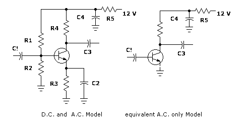
Figure 2.
Let's deal with the d.c. conditions first because we have to overcome one peculiar aspect of this type of transistor. It has to be turned on or have the base opened.
To do this, the base has to have a voltage applied to it which is approximately 0.65V higher than the voltage level at the emitter. In fact using this property allows a transistor to be used as a simple switch. Better still, arrange about 20,000,000 of them the right way around and you get a Pentium III.
With class A amplifiers this is done by biasing the transistor for d.c. conditions. Like this:
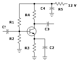
Figure 3.
Here we have our customary 12V d.c. power supply. We have a resistor from supply to base and another from base to ground. There is also a resistor from supply to collector as well as one from emitter to ground. What do these resistors do?.
Dealing with the pair associated with the base i.e. R1 and R2, they form a voltage divider network. The ratio of :
[R2/(R1 + R2)] * 12V = Base voltage (d.c.)
if we use 82K for R1 and 39K for R2 we would get a base voltage of
[39K/(82K + 39K)] * 12V = 3.87V (d.c.)
also the current flowing through these base resistors (ignoring any current into the base) is - from ohms law -
Ib = 12/ (R1 + R2) = 0.1 mA (rounding up slightly)
Now different people have different ideas but I'm a big believer in the theory that the current through the emitter should be between 5 - 10 times that of the base current. Let's pick a ratio of about midway, 7 i.e 0.7 mA for emitter current.
Of course if a higher emitter current was required then simply jack up your base current to maintain the approximate ratio.
Remember we said the base had to be 0.65V higher than the emitter?. Well if we have a base voltage (calculated above) of 3.87V and it is 0.65V higher than the emitter then the emitter must be (3.87 - 0.65) which is 3.22V. If we have also said that the emitter current is 0.7 mA then it follows the emitter resistor R3 must be - again Ohms Law -
Re = 3.22/.0007A = 4600 ohms or near enough to 4K7
If you are worrying about me jumping from 4600 ohms to the nearest standard, which is 4K7 or 4700 ohms, then keep things in perspective. Most resistors, capacitors in these circuits are about 5% or worse tolerance.
This then leaves the resistor from 12V supply to collector, R4.
This is called the load resistor. It could (at r.f.) easily be a choke, a transformer or a resonant circuit. For the moment we are hanging in at a.c., sort of working around audio frequencies but the same principles apply to r.f.
Now IF 0.7 mA is flowing (at d.c.) through the emitter then it must also flow through the collector. Also if our supply is 12V and the emitter voltage is 3.22V then the voltage at the collector must be:
Vcc - (Ic * RL) Where RL is in fact R4 or
12V - (0.0007A * R4)
If we elect to have a load resistor of 6800 ohms or 6K8 for R4 what happens?. Well all we have concentrated on so far - in a long winded way - is the d.c. conditions. What about a.c.? Now here is the pointy end of the stick. Remember I said a.c., meaning the usual audio frequencies but the same principles apply to r.f.
Firstly we need a coupling capacitor from the previous stage as well as a coupling capacitor at the output. These are C1 and C3 respectively. Their sole function is to block d.c. so that d.c. voltages in this stage do not transfer to adjacent stages. Usually we look for a very low reactance (Xc) at the frequency of interest so that frequency is not impeded in the transfer. A capacitor will pass a.c. or r.f. but not d.c.
A capacitor of 0.82 uF has a reactance of about 650 ohms at 300 Hz and 65 ohms at 3000 Hz. These being the two limits of audio frequencies for communications purposes. These values are considered low enough to use this capacitor here. Of course a higher value can be used but then you get into electrolytic types and polarity must be observed.
If this were a hi-fi type amplifier then you would certainly use higher values. On the other hand with communications receivers anything which reduces 50/60 Hz mains hum should be used so we tend to go for the lower values.
Looking back to the beginning we note that for a.c. or r.f. purposes the emitter should be grounded. I say should be, because if at a.c. there exists a resistor to ground then the gain suffers because of "emitter degeneration". Later we will take advantage of this in another circuit employing feedback.
For the present we need a grounded emitter at a.c. How is this achieved? Simple, by-pass the emitter resistor with another capacitor, C2 of the same or similar value to C1 and C3. This capacitor has the effect of making the emitter resistor R3 invisible for a.c. or r.f. purposes.
The last capacitor, C4 (again the same or higher in value) is from the 12V d.c. supply to ground. This has the effect in conjunction with R5 in the power supply line of decoupling the supply. This resistor might have a small value of say 33 ohms.
This means any a.c. or r.f in our amplifier section gets shunted to ground and does not pass along the d.c. power bus line to contaminate other stages. Similarly no contamination from other stages should ever get into our stage (well we can always live in hope - only joking).
So just what happens now that we have surrounded our transistor with resistors and capacitors?.
Well first of all what is the likely input impedance (that "I" word again) of our little amplifier?. Some engineers could write a whole text book on that topic alone. For our purposes we will use the following approximation:
Z in or R in = [25 * Beta (ac)] / Ie (mA)
This means 25 times the a.c. or r.f. beta, divided by the emitter current in milliamps.
Now if this was an r.f. amplifier we could approximate the r.f. beta by dividing the Ft by the frequency of operation. Our 2N2222A transistor has according to the specs earlier, a d.c. beta (Hfe) of 100 but at a collector current of 150 mA. As I said I've measured wide variations. At r.f., the specs say an Ft of 300 Mhz and if the amplifier was used at about 7 Mhz we could use an approximation for r.f. beta of 300/7 or about 40. But our present example is at audio frequencies where I would approximate a figure of 90. Substituting we get:
Z in or R in = [25 * 90] / 0.7 (mA) = 3300 or 3K3
This figure would be affected by the parallel combination of R1 and R2 but being quite large in comparison, can be ignored in this particular example.
Let us agree on a net input impedance of 3000 ohms or 3K. What if a signal of 10 millivolts a.c. were applied to the input of our amplifier?. In the base we would have (using ohms law) an a.c. current of 0.01/3000 or 3.3 uA flowing (that is 3.3 millionth of an amp).
If our a.c. beta was 90 then we may assume our collector current would vary by 90 * 3.3 uA or 300 uA. Now this amplified current at an a.c. rate passes through our load resistor R4, or 6800 ohms or 6K8. Again using nothing more than ohms law we find 300uA * 6800 = 2.04 volt swing. The small signal voltage gain is 2.04/.01 or 204. This is a gain of 46 dB, a high and possible unstable figure.
Looking a lot more closely at R4, because we had (under no signal conditions) a standing collector current through our transistor of 0.7 mA there must have been (again ohms law) a voltage drop across it of 6800 * 000.7 or 4.76 volts. Therefore measuring the voltage on our collector we would have had (12V - 4.76V) or 7.24 volts.
Under our 10 millivolts signal conditions that voltage would have swung plus and minus the amplified signal of 2.04 volts. Being an alternating variation or a.c. it is able to pass through coupling capacitor C3 on to the next stage.
The main point is, if you have kept awake so far, is that you have now digested the basic principles of amplifier design. Now we will enter the realms of refinements and embellishments.
NEXT - Class A Amplifier Design - Part 2 - using emitter degeneration
Collin's Home Page Colin's Amateur Radio Page Colin's Snooker Page Colin's Guest Book Contact Me About Me
This Web page was last updated on Friday September 21, 2001
© 2001 Designed by Colin McCord