

Class A Amplifier Design - Part 3
|
|
|
|
Class A Amplifier Design - Part 3 |
|
Tip: print these pages out NOW! after loading.
This is quite a lengthy document and contains schematics as .gif files. Accordingly it may take some time to download - but well worth the wait. Please be patient.
How is this accomplished. Quite easy! Shunt feedback is accomplished by adding one resistor and a capacitor between collector and base of our transistor. For this exercise I'm going to go to an r.f. application and replace resistor R4 with a choke, it could easily be a transformer. Look at Figure 5 below.
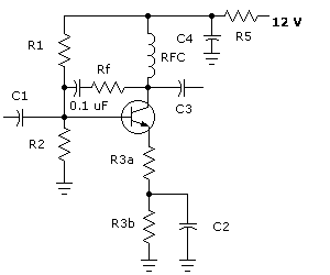
Figure 5.
Let's look at the choke RFC. What does it achieve for us?. Any inductor resists or opposes a change in current flowing in it. This has the effect of dumping any r.f. voltage through the C3 coupling capacitor.
TUNED CIRCUITS
What if we replace the RFC with a tuned circuit?. What benefits will accrue to us?.
we would introduce a measure of selectivity.
higher gain becomes possible
higher output power also becomes possible
Now let us review some our lessons from LC filters by examining a fairly basic LC resonant circuit as the load in place of our RFC.
Now here in figure 6 is a bog standard LC resonant circuit which comprises an inductor and a capacitor. You will note there has been a link coupling wound on the inductor.
Firstly the inductor could be of a fixed value such as one wound on a toroid or it could be a variable type similar to the ones found in receivers and used as IF transformers. Secondly the capacitor could be a fixed standard value one (e.g. 100 pF) or it could be a fixed standard value with an additional parallel capacitance in the form of a trimmer capacitor.
Either way we would have one variable element (inductor or capacitor) which allows us to tune to the frequency we want. Figure 6 uses a fixed capacitor with a parallel trimmer.
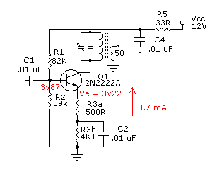
Figure 6
Here we are only mainly concerned here with the principle of a tuned circuit as a load. In this example we have a final load of 50 ohms connected to the output link coupling of our tuned circuit. Assume, just for discussion purposes, that in this example we needed a power output of 100 milliwatt from the amplifier and that we have available a power supply of 12V. Further,
Now:
2
* Po = [Vcc - Ve]2 / R
or [2* 0.1] = [12 - 3.22]2
/ R
or [2* 0.1] = [ 8.78 ]2
/ R
and R = 77 / 0.2
= 385 ohms
Therefore the load presented to the output of our amplifier needs to be 385 ohms. The impedance ratio is 385 / 50 or 7.7:1 and the turns ratio on the transformer (inductor) is the square root of that number or 2.775:1.
Again for discussion let us say we are designing this resonant circuit to work in the 40 metre amateur radio band. If you have done the LC filter tutorial you would know that the LC at 7.2 Mhz is about 490.
Now contrary to popular belief you will NOT get terribly impressive results from a single resonator circuit. That is really not the purpose of our resonator here. It's purpose is one of impedance transfer. We could just as easily used a low pass filter or even a high pass filter to achieve the same effect.
Let us choose an arbitrary inductance by selecting a suitable toroid core for the frequency. An Amidon T50-2 is a very such core. It has an AL factor of 49.
Assume for convenience that we wind 28 turns of #22 wire on this toroid. This many turns will occupy the entire winding area. What inductance results?
USE THIS FORMULA:
[ L / N2] = [ AL / 1002]
Therefore
[ L / 282] = [ 49 / 1002]
L = 3.84 uH
With such an inductor at 7.2 Mhz where we have said the LC is 490 we would need a total capacitance of about 128 pF to resonate with it. This would be provided by a fixed value of say 120 pf together with perhaps a 20 pF trimmer as depicted in figure 6. The inductor needed 28 turns primary and the turns ratio was 2.775:1 so our secondary turns to connect up to a 50 ohm load must be 10 turns. Before you go any further just review all that again.
Next we will have to check if our class A amplifier is going to remain linear and also prove our resonator circuit is no where near as flash as you might first think. More important, this particular design has potential deep flaws in it.
Above while calculating the load resistance for 100 milliwatt of power output I told you:
2 * Po = [Vcc - Ve]2 / RL
or
[2* 0.1] = [12 - 3.22]2 / RL
or
[2* 0.1] = [ 8.78 ]2 / RL
and
RL = 77 / 0.2
= 385 ohms
What I didn't tell you, but some advanced students might have worked out, the amplifier signal voltage could follow this excursion:-
on negative peaks down to zero before going into saturation and on positive peaks to 12V + 8.78V = 20.78V.
Obviously the only linear portion is plus and minus the potential swing of 8.78V or 17.56V Pk to Pk. To be able to do this our current must fluctuate from zero to twice our Idc value of 0.7 mA.
By using ohms law our load resistance, RL
RL = E pk / Idc
= 8.78 / .0007 A
= 12543 ohms
All right what has gone wrong? Let's re-work that equation to get the Idc we should have:
Idc = Vpk / RL
= 8.78 / 385
= 0.0223 A
OR
22.3 mA
Clearly I should have gone about this design another way. What I should do is make a list in the correct order of procedures or steps and calculate my components from those steps.
And if you think basic high school maths was a waste of time well check this out. There are no short cuts in life.
What output power do I want? - in this case 100 milliwatts or 0.1 W
What is my Vcc or D.C. power source? - In this case 12V dc
If I bias my transistor to say about .25 to .33 of supply then my base dc voltage (Vb) will lie between 3V and 4V both dc. [this is entirely my theory of design here - o.k.]
In which event my emitter voltage (Ve) is going to be 0.65 volts less than this or lie between 2.35V and 3.35V.
It follows that the maximum Vpk can only be Vcc - Ve or in this case again in between [12 - 2.35] and [12 - 3.35] which gives Vpk a range of 8.65 to 9.65 volts.
Now we know that RL is Vpk2 / 2 * Po so the possible range of loads must also lie in between 375 ohms and 465 ohms.
Again from above we also know that using ohms law, Idc = Vpk / RL, so our dc current must also be about 0.02 A or 20 mA. I would add a margin of +25% because I'm eccentric. So I will bias for around 25 mA
This much current to achieve the Ve's (dc) above mean our total emitter resistances must lie between a nice spread of 94 ohms total through to 135 ohms total [for the sleepyheads who can't fathom that Re = Ve / Idc]. Now 'boyz und girlz' that's a handy little range to play around in.
What about base current (Ib)? - said before I like about 1/5 to 1/7 of the emitter current to flow through the base resistance bias network. In this case we want about 3.5 to 5 mA through our base bias. Therefore R1 and R2 combined must total between 12v/.0035 and 12V/.005 or between 2400 ohms (min) and 3428 ohms (max). All we have to establish is the exact ratio, using standard values, to get the required Vb range of 25% to 33% of Vcc or 3V to 4V.
Let's play around a bit!. We don't want our lil' amp to suck do we?
Because we're asking for a bit of power (i.e. 0.1W) I'm inclined to go toward the lower Vb figure of 25% which gives a resistance ratio for R1/R2 of 3:1. Using these figures we could go, using standard values, 2400 ohms for R1 and 820 ohms for R2 (total of 3320). Here Ib is 12V/3320 = .0036A or 3.6 mA and Vb = Ib * 680 = 2.96V near enough to 3V.
If Vb is 2.96 then Ve = Vb - 0.65 or 2.31V. If we want a collector current of 25 mA then total Re = Ve/Ic or 2.31/0.025 or 92 ohms.
Now what sort of load do we want?. Well 2 * Po = [Vcc - Ve]2/ RL,so it follows that RL= [Vcc - Ve]2/ [2 * Po] or RL= [12V - 2.31]2 / [2 * 0.1W] which is = [9.69]2 / [ 0.2W] = 469 ohms
If our ultimate load is 50 ohms then we need a transfer ratio of 469:50 or 9.38:1 and the transformer turns ratio is the square root of that number or 3.06:1
So what gain do we need from the stage?. Personally I'm not wrapped in the idea of screwing the max out of stages and I figure a voltage gain of about 8 would pull me up. This is about 18dB gain, i.e. [20 * log 8]
Now if we need a gain of around 8 what is the value of the unbypassed emitter resistor? Remember gain is roughly RL / Re. So Re is 469/8 or 58 ohms. The nearest standard is 56 ohms which we will use. If the total emitter resistances were 92 ohms then the bypassed Re = 92 - 56 or 36 ohms. We'll use the standard 39 ohms.
How about our load transformer? - It was O.K. before so we will re-use it. It had 28 turns of #22 wire on a T50-2 toroid. Our turns ratio has been amended to 3.06:1 so we wind 9 turns on the secondary.
Now here's what you get for your money in figure 7
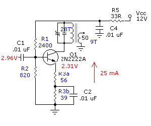
Figure 7
Another aspect which must be looked at is heatsinking. Our little 2N2222A is copping a lot of current and would require a decent heatsink. Actually I would consider using a T05 type transistor such as a 2N3866.
OUTPUT CIRCUIT
We do not have to use the above output LC circuit all the time because it's performance leaves much to be desired. Why?
We have an inductor of 3.84 uH used at 7.2 Mhz. It's inductive reactance is (2 * pi * 7.2 * 3.84) = 174 ohms. It would have an unloaded Q of about 160 i.e. Rp = QU * XL = 160 * 174 = 27840 ohms. This figure is the unloaded impedance. But we are connecting up to a 50 ohm load and are going to extract power from our little amplifier.
Now we have designed for a RL of 469 ohms which appears in parallel with the Rp of 27840. After calculation, [ Rp * RL ] / [ Rp + RL ], you should get a net load of 461 ohms. Our gain is now really 461 / Re or 461 / 56 = 8.2 BUT the loaded Q, QL is RL / XL or in this case QL = 461 / 174 = 2.65.
Alert students who have done and remembered the LC Filter Tutorial will know that our loaded bandwidth is Bw = Fo / QL or here it's 7200 Khz / 2.65 = 2716 Khz or 2.7 Mhz WIDE. In short it sux!.
What to do?. Well you can always go back and re-arrange all your design formula so you eventually get a better result. You could for example, connect the collector to a tap on the primary of the inductor, say about 9 turns up from the bottom of the schematic and reduce the secondary turns down to 3 turns. What effect does this have?.
The ultimate load is still 50 ohms. The unloaded Q and inductive reactance remain unaltered so Rp is still 27840. What would change is this. Firstly the primary:secondary turns ratio is now 28:3 which when squared transforms the primary impedance up to:
[ 28 / 3 ]2 * 50 = 4355 ohms
which again is in parallel with Rp of 27840 making a net RL of 3766 ohms.
QL is RL / XL
which is:
3766 / 174 = 21.64
a profound change is it not?. Therefore Bw = Fo / QL or here it's 7200 Khz / 21.64 = 332 Khz which is a more respectable figure. Of course you always believed you were going to get a narrow and razor sharp filter didn't you?.
Hey what sort of load does the transistor see?
Well a 28 turn primary which we just established has an impedance of 3766 ohms and the collector is tapped 9 turns from the bottom so it's as before 28:9 or
RL of 3766 ohms / [ 28 / 9 ]2 = 389 ohms
and gain is now 389 / 56 = 6.94 or nearly a quite respectable 17 dB voltage gain (ignoring any losses in the LC filter). That's about as thrilling as it gets.
LOW PASS FILTER APPROACH
Yes folks the output circuit could well have been a low pass LC filter designed to transform a desired RL of say 400 ohms to 50 ohms. The circuit would have looked like this.
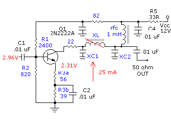
Figure 8
Rfc is not critical, it just resists rf getting into supply line, any thing with a reactance of about 20,000 ohms will do. Just ensure it can safely carry the necessary current. XC1, XC2 and XL are components calculated per low pass filter design. XL should be made variable (that's what the red line indicates).
When the output is terminated into an appropriate load and then monitored on a scope, the output change is quite profound whilst varying XL to proper resonance.
I've added two more resistors in, one in the collector to aid stability and one more in the supply line.
Remember we haven't discussed input impedance yet!
COMING SOON - Class A Amplifier Design - Part 4 - input / output impedances for previous amplifiers
Collin's Home Page Colin's Amateur Radio Page Colin's Snooker Page Colin's Guest Book Contact Me About Me
This Web page was last updated on Friday September 21, 2001
© 2001 Designed by Colin McCord